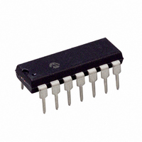
PIC16F616-E/P Microchip Technology, PIC16F616-E/P Datasheet - Page 44

PIC16F616-E/P
Manufacturer Part Number
PIC16F616-E/P
Description
IC PIC MCU FLASH 2KX14 14DIP
Manufacturer
Microchip Technology
Series
PIC® 16Fr
Datasheets
1.PIC12F609T-ISN.pdf
(26 pages)
2.PIC16F616T-ISL.pdf
(4 pages)
3.PIC16F616T-ISL.pdf
(214 pages)
4.PIC16F616T-ISL.pdf
(8 pages)
5.PIC16F616-ESL.pdf
(180 pages)
Specifications of PIC16F616-E/P
Program Memory Type
FLASH
Program Memory Size
3.5KB (2K x 14)
Package / Case
14-DIP (0.300", 7.62mm)
Core Processor
PIC
Core Size
8-Bit
Speed
20MHz
Peripherals
Brown-out Detect/Reset, POR, PWM, WDT
Number Of I /o
11
Ram Size
128 x 8
Voltage - Supply (vcc/vdd)
2 V ~ 5.5 V
Data Converters
A/D 8x10b
Oscillator Type
Internal
Operating Temperature
-40°C ~ 125°C
Processor Series
PIC16F
Core
PIC
Data Bus Width
8 bit
Data Ram Size
128 B
Maximum Clock Frequency
20 MHz
Number Of Programmable I/os
11
Number Of Timers
3
Maximum Operating Temperature
+ 125 C
Mounting Style
Through Hole
3rd Party Development Tools
52715-96, 52716-328, 52717-734
Development Tools By Supplier
PG164130, DV164035, DV244005, DV164005, PG164120, ICE2000
Minimum Operating Temperature
- 40 C
On-chip Adc
8-ch x 10-bit
Height
3.3 mm
Length
19.05 mm
Supply Voltage (max)
5.5 V
Supply Voltage (min)
2 V
Width
6.35 mm
Lead Free Status / RoHS Status
Lead free / RoHS Compliant
For Use With
MCP1631RD-DCPC1 - REF DES BATT CHARG OR LED DRIVERAC162083 - HEADER MPLAB ICD2 PIC16F616 8/14
Eeprom Size
-
Connectivity
-
Lead Free Status / Rohs Status
Lead free / RoHS Compliant
- PIC12F609T-ISN PDF datasheet
- PIC16F616T-ISL PDF datasheet #2
- PIC16F616T-ISL PDF datasheet #3
- PIC16F616T-ISL PDF datasheet #4
- PIC16F616-ESL PDF datasheet #5
- Current page: 44 of 214
- Download datasheet (4Mb)
PIC16F610/616/16HV610/616
4.3.5
The RC4 is configurable to function as one of the
following:
• a general purpose I/O
• a digital output from Comparator C2
• a digital output from the Enhanced CCP
FIGURE 4-8:
TABLE 4-2:
DS41288F-page 44
ANSEL
CCP1CON
CM1CON0
CM2CON0
PORTC
TRISC
Legend:
Note 1:
Data Bus
PORTC
PORTC
TRISC
TRISC
Note 1: PIC16F616/16HV616 only.
Name
CCPOUT/P1B
WR
WR
RD
Note
RD
CCP1M<3:0>
CCP1M<3:0>
2: Enabling both C2OUT and P1B will cause
C2OUT
(1)
C2OE
C2OE
1:
D
D
x = unknown, u = unchanged, – = unimplemented locations read as ‘0’. Shaded cells are not used by PORTC.
PIC16F616/HV616 only.
RC4/C2OUT/P1B
CK
CK
a conflict on RC4 and create unpredictable
results. Therefore, if C2OUT is enabled,
the ECCP can not be used in Half-Bridge
or Full-Bridge mode and vice-versa.
C1ON
C2ON
ANS7
P1M1
Port/Peripheral Select signals selects between
PORT data and peripheral output.
Bit 7
—
—
Q
Q
Q
Q
SUMMARY OF REGISTERS ASSOCIATED WITH PORTC
BLOCK DIAGRAM OF RC4
C1OUT
C2OUT
ANS6
P1M0
Bit 6
—
—
1
0
(1)
TRISC5
DC1B1
ANS5
C1OE
C2OE
Bit 5
RC5
TRISC4
(1)
C1POL
C2POL
DC1B0
ANS4
Bit 4
V
RC4
V
DD
SS
I/O Pin
CCP1M3
ANS3
TRISC3
Bit 3
RC3
—
—
(1)
CCP1M2
ANS2
TRISC2
4.3.6
The RC5 is configurable to function as one of the
following:
• a general purpose I/O
• a digital input/output for the Enhanced CCP
FIGURE 4-9:
Bit 2
C1R
C2R
RC2
PORTC
PORTC
Data bus
TRISC
TRISC
WR
WR
RD
RD
Note 1: PIC16F616/16HV616 only.
(1)
Note 1:
CCP1M1
To Enhanced CCP
TRISC1
D
D
C1CH1
C2CH1
ANS1
CK
CK
Bit 1
RC1
RC5/CCP1
PIC16F616/16HV616 only.
Q
Q
Q
Q
CCP1M0 0000 0000 0000 0000
TRISC0
C1CH0
C2CH0
CCP1OUT
ANS0
Bit 0
RC0
BLOCK DIAGRAM OF RC5
PIN
© 2009 Microchip Technology Inc.
(1)
P1A
/P1A
CCP1OUT
(1)
1111 1111 1111 1111
0000 -000 0000 -000
0000 -000 0000 -000
--xx 00xx --uu 00uu
--11 1111 --11 1111
POR, BOR
/
Enable
Value on
(1)
1
0
(1)
V
V
Value on
all other
DD
Resets
SS
(1)
I/O Pin
Related parts for PIC16F616-E/P
Image
Part Number
Description
Manufacturer
Datasheet
Request
R

Part Number:
Description:
3.5KB Flash, 128B RAM, 18 I/O, CLC, CWG, DDS, 10-bit ADC 20 QFN 4x4mm TUBE
Manufacturer:
Microchip Technology
Datasheet:

Part Number:
Description:
3.5KB Flash, 128B RAM, 18 I/O, CLC, CWG, DDS, 10-bit ADC 20 PDIP .300in TUBE
Manufacturer:
Microchip Technology
Datasheet:

Part Number:
Description:
3.5KB Flash, 128B RAM, 18 I/O, CLC, CWG, DDS, 10-bit ADC 20 SOIC .300in TUBE
Manufacturer:
Microchip Technology
Datasheet:

Part Number:
Description:
3.5KB Flash, 128B RAM, 18 I/O, CLC, CWG, DDS, 10-bit ADC 20 SSOP .209in TUBE
Manufacturer:
Microchip Technology
Datasheet:

Part Number:
Description:
3.5KB Flash, 128B RAM, 18 I/O, CLC, CWG, DDS, 10-bit ADC 20 QFN 4x4mm TUBE
Manufacturer:
Microchip Technology
Datasheet:

Part Number:
Description:
3.5KB Flash, 128B RAM, 18 I/O, CLC, CWG, DDS, 10-bit ADC 20 PDIP .300in TUBE
Manufacturer:
Microchip Technology
Datasheet:

Part Number:
Description:
3.5KB Flash, 128B RAM, 18 I/O, CLC, CWG, DDS, 10-bit ADC 20 SOIC .300in TUBE
Manufacturer:
Microchip Technology
Datasheet:

Part Number:
Description:
3.5KB Flash, 128B RAM, 18 I/O, CLC, CWG, DDS, 10-bit ADC 20 SSOP .209in TUBE
Manufacturer:
Microchip Technology
Datasheet:

Part Number:
Description:
3.5KB Flash, 128B RAM, 18 I/O, CLC, CWG, DDS, 10-bit ADC 20 QFN 4x4mm T/R
Manufacturer:
Microchip Technology
Datasheet:

Part Number:
Description:
3.5KB Flash, 128B RAM, 18 I/O, CLC, CWG, DDS, 10-bit ADC 20 SOIC .300in T/R
Manufacturer:
Microchip Technology
Datasheet:

Part Number:
Description:
3.5KB Flash, 128B RAM, 18 I/O, CLC, CWG, DDS, 10-bit ADC 20 SSOP .209in T/R
Manufacturer:
Microchip Technology
Datasheet:

Part Number:
Description:
3.5KB Flash, 128B RAM, 18 I/O, CLC, CWG, DDS, 10-bit ADC 20 QFN 4x4mm TUBE
Manufacturer:
Microchip Technology
Datasheet:

Part Number:
Description:
3.5KB Flash, 128B RAM, 18 I/O, CLC, CWG, DDS, 10-bit ADC 20 PDIP .300in TUBE
Manufacturer:
Microchip Technology
Datasheet:

Part Number:
Description:
3.5KB Flash, 128B RAM, 18 I/O, CLC, CWG, DDS, 10-bit ADC 20 SOIC .300in TUBE
Manufacturer:
Microchip Technology
Datasheet:

Part Number:
Description:
3.5KB Flash, 128B RAM, 18 I/O, CLC, CWG, DDS, 10-bit ADC 20 SSOP .209in TUBE
Manufacturer:
Microchip Technology
Datasheet:


