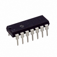
PIC16F616-E/P Microchip Technology, PIC16F616-E/P Datasheet - Page 47

PIC16F616-E/P
Manufacturer Part Number
PIC16F616-E/P
Description
IC PIC MCU FLASH 2KX14 14DIP
Manufacturer
Microchip Technology
Series
PIC® 16Fr
Datasheets
1.PIC12F609T-ISN.pdf
(26 pages)
2.PIC16F616T-ISL.pdf
(4 pages)
3.PIC16F616T-ISL.pdf
(214 pages)
4.PIC16F616T-ISL.pdf
(8 pages)
5.PIC16F616-ESL.pdf
(180 pages)
Specifications of PIC16F616-E/P
Program Memory Type
FLASH
Program Memory Size
3.5KB (2K x 14)
Package / Case
14-DIP (0.300", 7.62mm)
Core Processor
PIC
Core Size
8-Bit
Speed
20MHz
Peripherals
Brown-out Detect/Reset, POR, PWM, WDT
Number Of I /o
11
Ram Size
128 x 8
Voltage - Supply (vcc/vdd)
2 V ~ 5.5 V
Data Converters
A/D 8x10b
Oscillator Type
Internal
Operating Temperature
-40°C ~ 125°C
Processor Series
PIC16F
Core
PIC
Data Bus Width
8 bit
Data Ram Size
128 B
Maximum Clock Frequency
20 MHz
Number Of Programmable I/os
11
Number Of Timers
3
Maximum Operating Temperature
+ 125 C
Mounting Style
Through Hole
3rd Party Development Tools
52715-96, 52716-328, 52717-734
Development Tools By Supplier
PG164130, DV164035, DV244005, DV164005, PG164120, ICE2000
Minimum Operating Temperature
- 40 C
On-chip Adc
8-ch x 10-bit
Height
3.3 mm
Length
19.05 mm
Supply Voltage (max)
5.5 V
Supply Voltage (min)
2 V
Width
6.35 mm
Lead Free Status / RoHS Status
Lead free / RoHS Compliant
For Use With
MCP1631RD-DCPC1 - REF DES BATT CHARG OR LED DRIVERAC162083 - HEADER MPLAB ICD2 PIC16F616 8/14
Eeprom Size
-
Connectivity
-
Lead Free Status / Rohs Status
Lead free / RoHS Compliant
REGISTER 5-1:
TABLE 5-1:
© 2007 Microchip Technology Inc.
TMR0
INTCON
OPTION_REG
TRISA
Legend: – = Unimplemented locations, read as ‘0’, u = unchanged, x = unknown. Shaded cells are not used by the
bit 7
Legend:
R = Readable bit
-n = Value at POR
bit 7
bit 6
bit 5
bit 4
bit 3
bit 2-0
R/W-1
RAPU
Name
Timer0 module.
RAPU: PORTA Pull-up Enable bit
1 = PORTA pull-ups are disabled
0 = PORTA pull-ups are enabled by individual PORT latch values
INTEDG: Interrupt Edge Select bit
1 = Interrupt on rising edge of INT pin
0 = Interrupt on falling edge of INT pin
T0CS: TMR0 Clock Source Select bit
1 = Transition on T0CKI pin
0 = Internal instruction cycle clock (F
T0SE: TMR0 Source Edge Select bit
1 = Increment on high-to-low transition on T0CKI pin
0 = Increment on low-to-high transition on T0CKI pin
PSA: Prescaler Assignment bit
1 = Prescaler is assigned to the WDT
0 = Prescaler is assigned to the Timer0 module
PS<2:0>: Prescaler Rate Select bits
Timer0 Modules Register
RAPU INTEDG
SUMMARY OF REGISTERS ASSOCIATED WITH TIMER0
Bit 7
INTEDG
GIE
R/W-1
—
OPTION_REG: OPTION REGISTER
BIT VALUE
PEIE
Bit 6
000
001
010
011
100
101
110
111
—
W = Writable bit
‘1’ = Bit is set
R/W-1
T0CS
TRISA5 TRISA4 TRISA3 TRISA2 TRISA1 TRISA0 --11 1111 --11 1111
T0CS
Bit 5
TMR0 RATE
T0IE
1 : 2
1 : 4
1 : 8
1 : 16
1 : 32
1 : 64
1 : 128
1 : 256
PIC16F610/616/16HV610/616
T0SE
INTE
Bit 4
R/W-1
T0SE
Preliminary
WDT RATE
1 : 1
1 : 2
1 : 4
1 : 8
1 : 16
1 : 32
1 : 64
1 : 128
OSC
RAIE
Bit 3
PSA
/4)
U = Unimplemented bit, read as ‘0’
‘0’ = Bit is cleared
R/W-1
PSA
Bit 2
T0IF
PS2
INTF
Bit 1
PS1
R/W-1
PS2
RAIF
Bit 0
PS0
x = Bit is unknown
xxxx xxxx uuuu uuuu
0000 0000 0000 0000
1111 1111 1111 1111
POR, BOR
Value on
R/W-1
PS1
DS41288C-page 45
Value on
all other
Resets
R/W-1
PS0
bit 0


