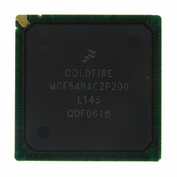
MCF5484CZP200 Freescale Semiconductor, MCF5484CZP200 Datasheet - Page 16
MCF5484CZP200
Manufacturer Part Number
MCF5484CZP200
Description
IC MPU 32BIT COLDF 388-PBGA
Manufacturer
Freescale Semiconductor
Series
MCF548xr
Datasheet
1.MCF5480CVR166.pdf
(34 pages)
Specifications of MCF5484CZP200
Core Processor
Coldfire V4E
Core Size
32-Bit
Speed
200MHz
Connectivity
CAN, EBI/EMI, Ethernet, I²C, SPI, UART/USART, USB
Peripherals
DMA, PWM, WDT
Number Of I /o
99
Program Memory Type
ROMless
Ram Size
32K x 8
Voltage - Supply (vcc/vdd)
1.43 V ~ 1.58 V
Oscillator Type
External
Operating Temperature
-40°C ~ 85°C
Package / Case
388-BGA
Program Memory Size
64KB
Cpu Speed
200MHz
Embedded Interface Type
I2C, UART, DMA
Digital Ic Case Style
BGA
No. Of Pins
388
Supply Voltage Range
3V To 3.6V, 1.43V To 1.58V
Rohs Compliant
No
For Use With
M5485EVBGHSE - KIT DEV GHS FOR M5485EVBM5485EVBGHS - KIT DEV GHS FOR M5485EVBM5485BFEE - MODULE MCF5485 FIRE ENGINEM5485AFEE - MODULE MCF5485 FIRE ENGINEM5485AFE - MODULE MCF5485 FIRE ENGINEM5484GFEE - MODULE M5484 FIRE ENGINEM5484LITEKITE - KIT DEV FOR MCF548X FAMILY
Lead Free Status / RoHS Status
Contains lead / RoHS non-compliant
Eeprom Size
-
Program Memory Size
-
Data Converters
-
Available stocks
Company
Part Number
Manufacturer
Quantity
Price
Company:

Part Number:
MCF5484CZP200
Manufacturer:
Exar
Quantity:
100
Company:
Part Number:
MCF5484CZP200
Manufacturer:
FREESCAL
Quantity:
185
Company:
Part Number:
MCF5484CZP200
Manufacturer:
Freescale Semiconductor
Quantity:
10 000


SDRAM Bus
16
1
2
3
4
5
6
7
8
Symbol
The frequency of operation is 2x or 4x the CLKIN frequency of operation. The MCF548X supports a single external reference
clock (CLKIN). This signal defines the frequency of operation for FlexBus and PCI, but SDRAM clock operates at the same
frequency as the internal bus clock. Please see the PLL chapter of the MCF548X Reference Manual for more information on
setting the SDRAM clock rate.
SDCLK is one SDRAM clock in (ns).
Pulse width high plus pulse width low cannot exceed min and max clock period.
Pulse width high plus pulse width low cannot exceed min and max clock period.
SDR_DQS is designed to pulse 0.25 clock before the rising edge of the memory clock. This is a guideline only. Subtle
variation from this guideline is expected. SDR_DQS only pulses during a read cycle and one pulse occurs for each data beat.
SDR_DQS is designed to pulse 0.25 clock before the rising edge of the memory clock. This spec is a guideline only. Subtle
variation from this guideline is expected. SDR_DQS only pulses during a read cycle and one pulse occurs for each data beat.
The SDR_DQS pulse is designed to be 0.5 clock in width. The timing of the rising edge is most important. The falling edge
does not affect the memory controller.
Because a read cycle in SDR mode uses the DQS circuit within the MCF548X, it is most critical that the data valid window
be centered 1/4 clk after the rising edge of DQS. Ensuring that this happens results in successful SDR reads. The input setup
spec is provided as guidance.
SD10
SD11
SD12
SD13
SD1
SD2
SD3
SD4
SD5
SD6
SD7
SD8
SD9
Frequency of Operation
Clock Period (t
Clock Skew (t
Pulse Width High (t
Pulse Width Low (t
Address, CKE, CAS, RAS, WE, BA, CS - Output Valid (t
Address, CKE, CAS, RAS, WE, BA, CS - Output Hold (t
SDRDQS Output Valid (t
SDDQS[3:0] input setup relative to SDCLK (t
SDDQS[3:0] input hold relative to SDCLK (t
Data Input Setup relative to SDCLK (reference only) (t
Data Input Hold relative to SDCLK (reference only) (t
Data and Data Mask Output Valid (t
Data and Data Mask Output Hold (t
SK
CK
)
)
CKL
CKH
Characteristic
)
)
DQSOV
MCF548x ColdFire
Table 11. SDR Timing Specifications
)
DH
DV
)
)
DQSIH
DQSIS
®
Microprocessor, Rev. 4
)
)
DIH
DIS
CMH
CMV
)
)
)
)
0.25 × SDCLK 0.40 × SDCLK
0.25 × SDCLK
Does not apply. 0.5 SDCLK fixed width.
7.52
0.45
0.45
Min
2.0
1.0
1.5
0
0.5 × SDCLK +
0.75 × SDCLK
Self timed
+0.500ns
1.0ns
TBD
Max
0.55
0.55
133
12
Freescale Semiconductor
SDCLK
SDCLK
Unit
Mhz
ns
ns
ns
ns
ns
ns
ns
ns
ns
Notes
1
2
3
4
5
6
7
8
Related parts for MCF5484CZP200
Image
Part Number
Description
Manufacturer
Datasheet
Request
R

Part Number:
Description:
Manufacturer:
Freescale Semiconductor, Inc
Datasheet:
Part Number:
Description:
Manufacturer:
Freescale Semiconductor, Inc
Datasheet:
Part Number:
Description:
Manufacturer:
Freescale Semiconductor, Inc
Datasheet:
Part Number:
Description:
Manufacturer:
Freescale Semiconductor, Inc
Datasheet:
Part Number:
Description:
Manufacturer:
Freescale Semiconductor, Inc
Datasheet:
Part Number:
Description:
Manufacturer:
Freescale Semiconductor, Inc
Datasheet:
Part Number:
Description:
Manufacturer:
Freescale Semiconductor, Inc
Datasheet:
Part Number:
Description:
Manufacturer:
Freescale Semiconductor, Inc
Datasheet:
Part Number:
Description:
Manufacturer:
Freescale Semiconductor, Inc
Datasheet:
Part Number:
Description:
Manufacturer:
Freescale Semiconductor, Inc
Datasheet:
Part Number:
Description:
Manufacturer:
Freescale Semiconductor, Inc
Datasheet:
Part Number:
Description:
Manufacturer:
Freescale Semiconductor, Inc
Datasheet:
Part Number:
Description:
Manufacturer:
Freescale Semiconductor, Inc
Datasheet:
Part Number:
Description:
Manufacturer:
Freescale Semiconductor, Inc
Datasheet:
Part Number:
Description:
Manufacturer:
Freescale Semiconductor, Inc
Datasheet: