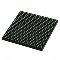
MCIMX513DJM8C Freescale Semiconductor, MCIMX513DJM8C Datasheet - Page 48

MCIMX513DJM8C
Manufacturer Part Number
MCIMX513DJM8C
Description
MULTIMEDIA PROC 529-LFBGA
Manufacturer
Freescale Semiconductor
Series
i.MX51r
Specifications of MCIMX513DJM8C
Core Processor
ARM Cortex-A8
Core Size
32-Bit
Speed
800MHz
Connectivity
1-Wire, EBI/EMI, Ethernet, I²C, IrDA, MMC, SPI, SSI, UART/USART, USB OTG
Peripherals
DMA, I²S, LCD, POR, PWM, WDT
Number Of I /o
128
Program Memory Type
ROMless
Ram Size
128K x 8
Voltage - Supply (vcc/vdd)
0.8 V ~ 1.15 V
Oscillator Type
External
Operating Temperature
-20°C ~ 85°C
Package / Case
529-LFBGA
Processor Series
i.MX51
Core
ARM Cortex A8
Data Bus Width
32 bit
Program Memory Size
36 KB
Data Ram Size
128 KB
Interface Type
I2C, SPI, SSI, UART, USB
Maximum Clock Frequency
200 MHz
Number Of Timers
5
Operating Supply Voltage
0.8 V to 1.15 V
Maximum Operating Temperature
+ 85 C
Mounting Style
SMD/SMT
3rd Party Development Tools
MDK-ARM, RL-ARM, ULINK2
Development Tools By Supplier
MCIMX51EVKJ
Minimum Operating Temperature
- 20 C
Lead Free Status / RoHS Status
Lead free / RoHS Compliant
Eeprom Size
-
Program Memory Size
-
Data Converters
-
Lead Free Status / Rohs Status
Lead free / RoHS Compliant
- Current page: 48 of 200
- Download datasheet (6Mb)
1
2
3
4
5
Electrical Characteristics
4.6.5
Table 48
4.6.6
This section provides the relative timing requirements among different signals of NFC at the module level
in the different operational modes.
Timing parameters in
(asymmetric mode) using two Flash clock cycles per one access of RE_B and WE_B.
Timing parameters in
NFC mode using one Flash clock cycle per one access of RE_B and WE_B.
48
Reference clock frequency range
Reference clock frequency range after
pre-divider
Output clock frequency range (dpdck_2)
Pre-division factor
Multiplication factor integer part
Multiplication factor numerator
Multiplication factor denominator
Output Duty Cycle
Frequency lock time
(FOL mode or non-integer MF)
Phase lock time
Frequency jitter
Phase jitter (peak value)
Power dissipation
Device input range cannot exceed the electrical specifications of the CAMP, see
The values specified here are internal to DPLL. Inside the DPLL, a “1” is added to the value specified by the user.Therefore,
the user has to enter a value “1” less than the desired value at the inputs of DPLL for PDF and MFD.
The maximum total multiplication factor (MFI + MFN/MFD) allowed is 15.Therefore, if the MFI value is 15, MFN value must be
zero.
T
mode is 398 cycles of divided reference clock when DPLL starts after full reset.
Tdck is the time period of the output clock, dpdck_2.
dpdref
is the time period of the reference clock after predivider.According to the specification, the maximum lock time in FOL
shows the DPLL electical parameters.
DPLL Electrical Parameters
NAND Flash Controller (NFC) Parameters
Parameter
5
(peak value)
2
4
i.MX51 Applications Processors for Consumer and Industrial Products, Rev. 4
Figure
Figure
3
2
1
14,
14, through
Figure
Table 48. DPLL Electrical Parameters
FPL mode, integer and fractional MF
Should be less than denominator
f
dvdd = 1.2 V
f
dvdd = 1.2 V
dck
dck
= 300 MHz @ avdd = 1.8 V,
= 650 MHz @ avdd = 1.8 V,
15,
Test Conditions/Remarks
Figure
Figure
17,
16,
—
—
—
—
—
—
—
—
—
—
Figure
Figure
19, and
18,
Figure
Table 50
–67108862
Table
48.5
Min
300
19, and
10
10
—
—
—
—
—
1
5
1
47.
show the default NFC mode
Table 50
0.02
Typ
2.0
50
—
—
—
—
—
—
—
—
—
—
Freescale Semiconductor
0.65 (avdd)
0.92 (dvdd)
1.98 (avdd)
1.8 (dvdd)
67108862
67108863
show symmetric
1025
Max
51.5
0.04
100
398
100
3.5
40
16
15
T
MHz
MHz
MHz
d
Unit
T
mW
pdref
—
—
—
—
ns
%
µ
dck
s
Related parts for MCIMX513DJM8C
Image
Part Number
Description
Manufacturer
Datasheet
Request
R
Part Number:
Description:
MCIMX-LVDS1
Manufacturer:
Freescale Semiconductor
Datasheet:
Part Number:
Description:
Manufacturer:
Freescale Semiconductor, Inc
Datasheet:
Part Number:
Description:
Manufacturer:
Freescale Semiconductor, Inc
Datasheet:
Part Number:
Description:
Manufacturer:
Freescale Semiconductor, Inc
Datasheet:
Part Number:
Description:
Manufacturer:
Freescale Semiconductor, Inc
Datasheet:
Part Number:
Description:
Manufacturer:
Freescale Semiconductor, Inc
Datasheet:
Part Number:
Description:
Manufacturer:
Freescale Semiconductor, Inc
Datasheet:
Part Number:
Description:
Manufacturer:
Freescale Semiconductor, Inc
Datasheet:
Part Number:
Description:
Manufacturer:
Freescale Semiconductor, Inc
Datasheet:
Part Number:
Description:
Manufacturer:
Freescale Semiconductor, Inc
Datasheet:
Part Number:
Description:
Manufacturer:
Freescale Semiconductor, Inc
Datasheet:
Part Number:
Description:
Manufacturer:
Freescale Semiconductor, Inc
Datasheet:
Part Number:
Description:
Manufacturer:
Freescale Semiconductor, Inc
Datasheet:
Part Number:
Description:
Manufacturer:
Freescale Semiconductor, Inc
Datasheet:
Part Number:
Description:
Manufacturer:
Freescale Semiconductor, Inc
Datasheet:


