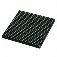
MCIMX513DJM8C Freescale Semiconductor, MCIMX513DJM8C Datasheet - Page 28

MCIMX513DJM8C
Manufacturer Part Number
MCIMX513DJM8C
Description
MULTIMEDIA PROC 529-LFBGA
Manufacturer
Freescale Semiconductor
Series
i.MX51r
Specifications of MCIMX513DJM8C
Core Processor
ARM Cortex-A8
Core Size
32-Bit
Speed
800MHz
Connectivity
1-Wire, EBI/EMI, Ethernet, I²C, IrDA, MMC, SPI, SSI, UART/USART, USB OTG
Peripherals
DMA, I²S, LCD, POR, PWM, WDT
Number Of I /o
128
Program Memory Type
ROMless
Ram Size
128K x 8
Voltage - Supply (vcc/vdd)
0.8 V ~ 1.15 V
Oscillator Type
External
Operating Temperature
-20°C ~ 85°C
Package / Case
529-LFBGA
Processor Series
i.MX51
Core
ARM Cortex A8
Data Bus Width
32 bit
Program Memory Size
36 KB
Data Ram Size
128 KB
Interface Type
I2C, SPI, SSI, UART, USB
Maximum Clock Frequency
200 MHz
Number Of Timers
5
Operating Supply Voltage
0.8 V to 1.15 V
Maximum Operating Temperature
+ 85 C
Mounting Style
SMD/SMT
3rd Party Development Tools
MDK-ARM, RL-ARM, ULINK2
Development Tools By Supplier
MCIMX51EVKJ
Minimum Operating Temperature
- 20 C
Lead Free Status / RoHS Status
Lead free / RoHS Compliant
Eeprom Size
-
Program Memory Size
-
Data Converters
-
Lead Free Status / Rohs Status
Lead free / RoHS Compliant
- Current page: 28 of 200
- Download datasheet (6Mb)
1
2
3
4
Electrical Characteristics
4.3.5
The DC Electrical Characteristics listed below are guaranteed using operating ranges per
otherwise noted.
28
Input Hysteresis
Schmitt trigger VT+
Schmitt trigger VT–
Input current (no pull-up/down)
Input current (22 kΩ Pull-up)
Input current (75 kΩ Pull-up)
Input current (100 kΩ Pull-up)
Input current (360 kΩ Pull-down)
Keeper Circuit Resistance
Low-level output voltage
High-Level DC input voltage
Low-Level DC input voltage
Input Hysteresis
Schmitt trigger VT+
Schmitt trigger VT–
I/O leakage current (no pull-up)
level through to the target DC level, VIL or VIH. Monotonic input transition time is from 0.1 ns to 1 s.
Overshoot and undershoot conditions (transitions above OVDD and below OVSS) on switching pads must be held below 0.6
V, and the duration of the overshoot/undershoot must not exceed 10% of the system clock cycle. Overshoot/undershoot must
be controlled through printed circuit board layout, transmission line impedance matching, signal line termination, or other
methods. Non-compliance to this specification may affect device reliability or cause permanent damage to the device.
Hysteresis of 250 mV is guaranteed over all operating conditions when hysteresis is enabled.
I/O leakage currents are listed in
To maintain a valid level, the transitioning edge of the input must sustain a constant slew rate (monotonic) from the current DC
Table 22. I
DC Electrical Characteristics
Parameter
I
2
C I/O DC Parameters
2
C Standard/Fast/High-Speed Mode Electrical Parameters for Low/Medium Drive Strength
See the errata for HS-I2C in i.MX51 Chip Errata document. The two
standard I
2,4
2,3
1,2
1,2
i.MX51 Applications Processors for Consumer and Industrial Products, Rev. 4
Table 21. UHVIO DC Electrical Characteristics (continued)
1
2
1
C modules have no errata.
Table
Symbol
VHYS
VT+
VT–
VIH
VIL
Vol
Iin
25.
Test Conditions
VI = OVDD or 0
Symbol
VHYS
VT+
VT–
Iol = 3 mA
Iin
Iin
Iin
Iin
Iin
—
—
—
—
—
—
NOTE
High voltage mode
Low voltage mode
Test Conditions
Vin = OVDD
Vin = OVDD
Vin = 0
Vin = 0
Vin = 0
Vin = 0
0.7 × OVDD
0.5 × OVDD
NA
—
—
0.25
Min
—
—
—
0
0.5OVDD
Typ
0.38
0.95
Min
—
—
—
—
—
—
—
—
—
—
—
—
—
—
0.3 × OVDD
0.5 × OVDD
See Note
Typ
17
—
—
—
—
—
—
—
—
Freescale Semiconductor
OVDD
Max
0.4
—
—
0.5 × OVDD
Table
See Note
3
Max
0.43
1.33
202
5.7
61
47
—
—
13, unless
Unit
4
—
V
V
V
V
V
V
Unit
kΩ
μA
μA
μA
μA
—
V
V
V
Related parts for MCIMX513DJM8C
Image
Part Number
Description
Manufacturer
Datasheet
Request
R
Part Number:
Description:
MCIMX-LVDS1
Manufacturer:
Freescale Semiconductor
Datasheet:
Part Number:
Description:
Manufacturer:
Freescale Semiconductor, Inc
Datasheet:
Part Number:
Description:
Manufacturer:
Freescale Semiconductor, Inc
Datasheet:
Part Number:
Description:
Manufacturer:
Freescale Semiconductor, Inc
Datasheet:
Part Number:
Description:
Manufacturer:
Freescale Semiconductor, Inc
Datasheet:
Part Number:
Description:
Manufacturer:
Freescale Semiconductor, Inc
Datasheet:
Part Number:
Description:
Manufacturer:
Freescale Semiconductor, Inc
Datasheet:
Part Number:
Description:
Manufacturer:
Freescale Semiconductor, Inc
Datasheet:
Part Number:
Description:
Manufacturer:
Freescale Semiconductor, Inc
Datasheet:
Part Number:
Description:
Manufacturer:
Freescale Semiconductor, Inc
Datasheet:
Part Number:
Description:
Manufacturer:
Freescale Semiconductor, Inc
Datasheet:
Part Number:
Description:
Manufacturer:
Freescale Semiconductor, Inc
Datasheet:
Part Number:
Description:
Manufacturer:
Freescale Semiconductor, Inc
Datasheet:
Part Number:
Description:
Manufacturer:
Freescale Semiconductor, Inc
Datasheet:
Part Number:
Description:
Manufacturer:
Freescale Semiconductor, Inc
Datasheet:


