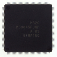
M30845FJGP#U3 Renesas Electronics America, M30845FJGP#U3 Datasheet - Page 19

M30845FJGP#U3
Manufacturer Part Number
M30845FJGP#U3
Description
IC M32C MCU FLASH 512K 144LQFP
Manufacturer
Renesas Electronics America
Series
M16C™ M32C/80r
Specifications of M30845FJGP#U3
Core Processor
M32C/80
Core Size
16/32-Bit
Speed
32MHz
Connectivity
CAN, I²C, IEBus, SIO, UART/USART
Peripherals
DMA, PWM, WDT
Number Of I /o
121
Program Memory Size
512KB (512K x 8)
Program Memory Type
FLASH
Ram Size
24K x 8
Voltage - Supply (vcc/vdd)
3 V ~ 5.5 V
Data Converters
A/D 34x10b, D/A 2x8b
Oscillator Type
Internal
Operating Temperature
-40°C ~ 85°C
Package / Case
144-LQFP
Lead Free Status / RoHS Status
Lead free / RoHS Compliant
Eeprom Size
-
Available stocks
Company
Part Number
Manufacturer
Quantity
Price
M
R
e
3
. v
2
I : Input
NOTES:
Table 1.6 Pin Description (100-Pin and 144-Pin Packages) (Continued)
Reference
Voltage Input
A/D Converter
D/A Converter
Intelligent I/O
CAN
I/O Ports
Input Port
C
Classsfication
1
2 .
8 /
1. V
1
4
G
J
CC2
u
o r
. l
u
0
O : Output
is not available in the 100-pin package. V
p
, 8
(
2
M
0
3
0
V
AN
AN0
AN2
AD
ANEX0
ANEX1
DA0, DA1
INPC1
INPC1
OUTC1
OUTC1
ISCLK0
ISCLK1
ISRXD0
ISRXD1
ISTXD0
ISTXD1
BE1
BE1
CAN0
CAN0
P0
P1
P2
P3
P4
P5
P6
P7
P9
P10
P8
P8
P8
___________
5
2
REF
Symbol
C
0
0
0
0
0
0
0
0
0
0
6
5
0
TRG
0
0
0
, P8
0
4
0
4
8 /
IN
OUT
to P0
to P1
to P2
to P3
to P4
to P5
to P6
to P7
to P9
to P8
to AN
to P10
to AN0
to AN2
to INPC1
to INPC1
to OUTC1
to OUTC1
IN
OUT
Page 17
, 4
7
M
7
7
7
7
7
7
7
7
7
4
I/O : Input and output
7
7
7
7
3
7
3
7
3
2
I/O Type
C
f o
I/O
I/O
I/O
I/O
I/O
I/O
8 /
O
O
O
O
O
O
O
I
I
I
I
I
I
I
I
I
I
I
8
4
5
) T
V
V
V
V
V
V
V
CC1
CC1
CC1
CC1
CC1
CC1
CC1
Voltage
Supply
-
V
V
V
V
V
V
V
V
V
V
V
V
V
V
V
V
/V
/V
/V
/V
/V
/V
/V
CC1
CC1
CC1
CC1
CC1
CC1
CC1
CC1
CC1
CC1
CC1
CC1
CC2
CC1
CC1
CC1
CC2 (1)
CC2 (1)
CC2 (1)
CC2 (1)
CC2 (1)
CC2 (1)
CC2 (1)
Applies reference voltage to the A/D converter and D/A converter
Analog input pins for the A/D converter
Input pin for an external A/D trigger
Extended analog input pin for the A/D converter and output pin in
external op-amp connection mode
Extended analog input pin for the A/D converter
Output pin for the D/A converter
Input pins for the time measurement function
Output pins for the waveform generating function
(OUTC1
Inputs and outputs the clock for the intellignet I/O communication
function
Inputs data for the intellignet I/O communication function
Outputs data for the intellignet I/O communication function
Inputs data for the intellignet I/O communication function
Outputs data for the intellignet I/O communication function
Input pin for the CAN communication function
Output pin for the CAN communication function
I/O ports for CMOS. Each port can be programmed for input or
output under the control of the direction register. An input port
can be set, by program, for a pull-up resistor available or for no
pull-up resister available in 4-bit units
I/O ports having equivalent functions to P0
(P7
I/O ports having equivalent functions to P0
Shares a pin with NMI. NMI input state can be got by reading P8
0
CC1
and P7
6
and OUTC1
only available.
1
are ports for the N-channel open drain output.)
7
assgined to P7
_______
_______
0
and P7
Function
1
are pins for the N-channel open drain output.)
1. Overview
5


