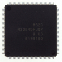
M30845FJGP#U3 Renesas Electronics America, M30845FJGP#U3 Datasheet - Page 18

M30845FJGP#U3
Manufacturer Part Number
M30845FJGP#U3
Description
IC M32C MCU FLASH 512K 144LQFP
Manufacturer
Renesas Electronics America
Series
M16C™ M32C/80r
Specifications of M30845FJGP#U3
Core Processor
M32C/80
Core Size
16/32-Bit
Speed
32MHz
Connectivity
CAN, I²C, IEBus, SIO, UART/USART
Peripherals
DMA, PWM, WDT
Number Of I /o
121
Program Memory Size
512KB (512K x 8)
Program Memory Type
FLASH
Ram Size
24K x 8
Voltage - Supply (vcc/vdd)
3 V ~ 5.5 V
Data Converters
A/D 34x10b, D/A 2x8b
Oscillator Type
Internal
Operating Temperature
-40°C ~ 85°C
Package / Case
144-LQFP
Lead Free Status / RoHS Status
Lead free / RoHS Compliant
Eeprom Size
-
Available stocks
Company
Part Number
Manufacturer
Quantity
Price
R
M
e
3
. v
2
I : Input
NOTES:
_______
Table 1.6 Pin Description (100-Pin and 144-Pin Packages) (Continued)
Main Clock Input
Main Clock Output
Sub Clock Input
Sub Clock Output
BCLK Output
Clock Output
______
INT Interrupt
Input
NMI Interrupt Input
Key Input Interrupt
Timer A
Timer B
Three-phase Motor
Control Timer Output
Serial I/O
I
Serial I/O
Special Function
C
Classsfication
1
2
C Mode
2 .
8 /
1. Bus control pins in M32C/84T cannot be used.
1
4
G
J
u
o r
. l
u
0
O : Output
, 8
p
(1)
(
2
M
0
_______
_______
X
X
X
X
BCLK
CLK
________
INT0 to INT2
________
INT3 to INT5
NMI
_____
KI
TA0
TA4
TA0
TA4
TB0
TB5
U, U, V, V,
W, W
_________
CTS0 to CTS4
_________
RTS0 to RTS4
CLK0 to CLK4
RxD0 to RxD4
TxD0 to TxD4
SDA0 to
SDA4
SCL0 to
SCL4
STxD0 to
STxD4
SRxD0 to
SRxD4
SS0 to SS4
0
3
5
2
IN
OUT
CIN
COUT
Symbol
0
___
C
___
to KI
OUT
OUT
IN
IN
IN
IN
OUT
8 /
_____
Page 16
to
to
, 4
________
________
_______
________
________
___
3
to
M
I/O : Input and output
3
I/O Type
2
C
I/O
I/O
I/O
I/O
f o
O
O
O
O
O
O
O
O
I
I
I
I
I
I
I
I
I
I
I
I
8 /
8
4
5
) T
Voltage
Supply
V
V
V
V
V
V
V
V
V
V
V
V
V
V
V
V
V
V
V
V
V
V
V
V
CC1
CC1
CC1
CC1
CC2
CC2
CC1
CC2
CC1
CC1
CC1
CC1
CC1
CC1
CC1
CC1
CC1
CC1
CC1
CC1
CC1
CC1
CC1
CC1
I/O pins for the main clock oscillation circuit. Connect a ceramic
resonator or crystal oscillator between X
external clock, apply it to X
I/O pins for the sub clock oscillation circuit. Connect a crystal
oscillator between X
apply it to X
Outputs BCLK signal
Outputs the clock having the same frequency as f
Input pins for the INT interrupt
Input pin for the NMI interrupt
Input pins for the key input interrupt
I/O pins for the timer A0 to A4
(TA0
Input pins for the timer A0 to A4
Input pins for the timer B0 to B5
Output pins for the three-phase motor control timer
Iutput pins for data transmission control
Output pins for data reception control
Inputs and outputs the transfer clock
Inputs serial data
Outputs serial data
(TxD2 is a pin for the N-channel open drain output.)
Inputs and outputs serial data
(SDA2 is a pin for the N-channel open drain output.)
Inputs and outputs the transfer clock
(SCL2 is a pin for the N-channel open drain output.)
Outputs serial data when slave mode is selected
(STxD2 is a pin for the N-channel open drain output.)
Inputs serial data when slave mode is selected
Input pins to control serial I/O special function
OUT
is a pin for the N-channel open drain output.)
CIN
and leave X
_______
______
CIN
and X
IN
COUT
Function
and leave X
COUT
open
. To apply external clock,
IN
OUT
and X
open
OUT
C
, f
. To apply
8
or f
1. Overview
32


