M30879FLGP#U3 Renesas Electronics America, M30879FLGP#U3 Datasheet - Page 63
M30879FLGP#U3
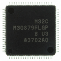
Manufacturer Part Number
M30879FLGP#U3
Description
IC M32C/87 MCU FLASH 100LQFP
Manufacturer
Renesas Electronics America
Series
M16C™ M32C/80r
Specifications of M30879FLGP#U3
Core Size
16/32-Bit
Program Memory Size
1MB (1M x 8)
Core Processor
M32C/80
Speed
32MHz
Connectivity
CAN, EBI/EMI, I²C, IEBus, IrDA, SIO, UART/USART
Peripherals
DMA, POR, PWM, WDT
Number Of I /o
85
Program Memory Type
FLASH
Ram Size
48K x 8
Voltage - Supply (vcc/vdd)
3 V ~ 5.5 V
Data Converters
A/D 26x10b; D/A 2x8b
Oscillator Type
Internal
Operating Temperature
-40°C ~ 85°C
Package / Case
100-LQFP
Controller Family/series
M32C
No. Of I/o's
85
Ram Memory Size
48KB
Cpu Speed
32MHz
No. Of Timers
2
Digital Ic Case Style
LQFP
Embedded Interface Type
CAN, I2C, UART
Rohs Compliant
Yes
Lead Free Status / RoHS Status
Lead free / RoHS Compliant
For Use With
R0K330879S001BE - KIT DEV RSK M32C/87R0K330879S000BE - KIT DEV RSK M32C/87
Eeprom Size
-
Lead Free Status / RoHS Status
Lead free / RoHS Compliant, Lead free / RoHS Compliant
Available stocks
Company
Part Number
Manufacturer
Quantity
Price

Part Number:
M30879FLGP#U3M30879FLGP#U5
Manufacturer:
Renesas Electronics America
Quantity:
10 000


M32C/87 Group (M32C/87, M32C/87A, M32C/87B)
REJ03B0127-0151 Rev.1.51 Jul 31, 2008
Page 61 of 85
Timing Requirements
(VCC1 = VCC2 = 4.2 to 5.5 V, VSS = 0 V, Topr = -20 to 85°C unless otherwise specified)
Table 5.28
NOTE:
tac1(RD-DB)
tac1(AD-DB)
tac2(RD-DB)
tac2(AD-DB)
tsu(DB-BCLK)
tsu(RDY-BCLK)
tsu(HOLD-BCLK)
th(RD-DB)
th(BCLK-RDY)
th(BCLK-HOLD)
td(BCLK-HLDA)
1. Values, which depend on BCLK frequency and external bus cycles, can be obtained from the following
Symbol
equations. Insert wait states or lower the operation frequency, f(BCLK), if the calculated value is negative.
tac1(RD-DB) =
tac1(AD-DB) =
tac2(RD-DB) =
tac2(AD-DB) =
Memory Expansion mode and Microprocessor Mode
Data input access time (RD standard)
Data input access time (AD standard, CS standard)
Data input access time (RD standard, when accessing a space with the
multiplexed bus)
Data input access time (AD standard, when accessing a space with the
multiplexed bus)
Data input setup time
RDY input setup time
HOLD input setup time
Data input hold time
RDY input hold time
HOLD input hold time
HLDA output delay time
f(BCLK) × 2
f(BCLK) × 2
f(BCLK) × 2
10
10
10
10
f(BCLK)
9
9
9
9
× m
× n
× m
× p
- 35 [ns] (if external bus cycle is a φ + b φ , m = (b × 2) + 1)
- 35 [ns] (if external bus cycle is a φ + b φ , n = a + b)
- 35 [ns] (if external bus cycle is a φ + b φ , m = (b × 2) - 1)
- 35 [ns] (if external bus cycle is a φ + b φ , p = {(a + b - 1) × 2} + 1)
Parameter
VCC1 = VCC2 = 5V
5. Electrical Characteristics
Min.
26
26
30
0
0
0
Standard
(note 1)
(note 1)
(note 1)
(note 1)
Max.
25
Unit
ns
ns
ns
ns
ns
ns
ns
ns
ns
ns
ns
Related parts for M30879FLGP#U3
Image
Part Number
Description
Manufacturer
Datasheet
Request
R

Part Number:
Description:
KIT STARTER FOR M16C/29
Manufacturer:
Renesas Electronics America
Datasheet:

Part Number:
Description:
KIT STARTER FOR R8C/2D
Manufacturer:
Renesas Electronics America
Datasheet:

Part Number:
Description:
R0K33062P STARTER KIT
Manufacturer:
Renesas Electronics America
Datasheet:

Part Number:
Description:
KIT STARTER FOR R8C/23 E8A
Manufacturer:
Renesas Electronics America
Datasheet:

Part Number:
Description:
KIT STARTER FOR R8C/25
Manufacturer:
Renesas Electronics America
Datasheet:

Part Number:
Description:
KIT STARTER H8S2456 SHARPE DSPLY
Manufacturer:
Renesas Electronics America
Datasheet:

Part Number:
Description:
KIT STARTER FOR R8C38C
Manufacturer:
Renesas Electronics America
Datasheet:

Part Number:
Description:
KIT STARTER FOR R8C35C
Manufacturer:
Renesas Electronics America
Datasheet:

Part Number:
Description:
KIT STARTER FOR R8CL3AC+LCD APPS
Manufacturer:
Renesas Electronics America
Datasheet:
Part Number:
Description:
KIT STARTER FOR RX610
Manufacturer:
Renesas Electronics America
Datasheet:

Part Number:
Description:
KIT STARTER FOR R32C/118
Manufacturer:
Renesas Electronics America
Datasheet:

Part Number:
Description:
KIT DEV RSK-R8C/26-29
Manufacturer:
Renesas Electronics America
Datasheet:

Part Number:
Description:
KIT STARTER FOR SH7124
Manufacturer:
Renesas Electronics America
Datasheet:

Part Number:
Description:
KIT STARTER FOR H8SX/1622
Manufacturer:
Renesas Electronics America
Datasheet:

Part Number:
Description:
KIT DEV FOR SH7203
Manufacturer:
Renesas Electronics America
Datasheet: