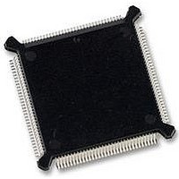
MC68332GCEH20 Freescale Semiconductor, MC68332GCEH20 Datasheet - Page 80

MC68332GCEH20
Manufacturer Part Number
MC68332GCEH20
Description
IC MCU 32BIT 20MHZ 132-PQFP
Manufacturer
Freescale Semiconductor
Series
M683xxr
Specifications of MC68332GCEH20
Core Processor
CPU32
Core Size
32-Bit
Speed
20MHz
Connectivity
EBI/EMI, SCI, SPI, UART/USART
Peripherals
POR, PWM, WDT
Number Of I /o
15
Program Memory Type
ROMless
Ram Size
2K x 8
Voltage - Supply (vcc/vdd)
4.5 V ~ 5.5 V
Oscillator Type
Internal
Operating Temperature
-40°C ~ 85°C
Package / Case
132-QFP
Controller Family/series
68K
No. Of I/o's
15
Ram Memory Size
2KB
Cpu Speed
20MHz
No. Of Timers
1
Embedded Interface Type
QSPI, SCI, UART
Digital Ic Case Style
PQFP
Rohs Compliant
Yes
Data Bus Width
32 bit
Data Ram Size
2 KB
Interface Type
QSPI, SCI, UART
Maximum Clock Frequency
20 MHz
Number Of Programmable I/os
15
Number Of Timers
16
Maximum Operating Temperature
+ 85 C
Mounting Style
SMD/SMT
Minimum Operating Temperature
- 40 C
Lead Free Status / RoHS Status
Lead free / RoHS Compliant
Eeprom Size
-
Program Memory Size
-
Data Converters
-
Lead Free Status / Rohs Status
Details
Available stocks
Company
Part Number
Manufacturer
Quantity
Price
Company:
Part Number:
MC68332GCEH20
Manufacturer:
Freescale Semiconductor
Quantity:
10 000
Part Number:
MC68332GCEH20
Manufacturer:
FREESCALE
Quantity:
20 000
SCCR1 — SCI Control Register 1
Bit 15 — Not Implemented
LOOPS — Loop Mode
WOMS — Wired-OR Mode for SCI Pins
ILT — Idle-Line Detect Type
PT — Parity Type
80
MOTOROLA
RESET:
Nominal Baud Rate
15
0
0
Writing a value of zero to SCBR disables the baud rate generator.
The following table lists the SCBR settings for standard and maximum baud rates using 16.78-MHz and
20.97-MHz system clocks.
SCCR1 contains SCI configuration parameters. The CPU can read and write this register at any time.
The SCI can modify RWU in some circumstances. In general, interrupts enabled by these control bits
are cleared by reading SCSR, then reading (receiver status bits) or writing (transmitter status bits)
SCDR.
LOOPS controls a feedback path on the data serial shifter. When loop mode is enabled, SCI transmitter
output is fed back into the receive serial shifter. TXD is asserted (idle line). Both transmitter and receiver
must be enabled before entering loop mode.
WOMS determines whether the TXD pin is an open-drain output or a normal CMOS output. This bit is
used only when TXD is an output. If TXD is used as a general-purpose input pin, WOMS has no effect.
When parity is enabled, PT determines whether parity is even or odd for both the receiver and the trans-
mitter.
Maximum Rate
0 = Normal SCI operation, no looping, feedback path disabled
1 = Test SCI operation, looping, feedback path enabled
0 = If configured as an output, TXD is a normal CMOS output.
1 = If configured as an output, TXD is an open-drain output.
0 = Short idle-line detect (start count on first one)
1 = Long idle-line detect (start count on first one after stop bit(s))
0 = Even parity
1 = Odd parity
19200
38400
76800
LOOPS WOMS
1200
2400
4800
9600
110
300
600
64*
14
0
13
0
ILT
12
0
Freescale Semiconductor, Inc.
16.78-MHz Clock
Actual Rate with
PT
11
For More Information On This Product,
0
524288.0
19418.1
37449.1
74898.3
1199.7
2405.0
4810.0
9532.5
110.0
299.9
599.9
64.0
PE
10
0
Go to: www.freescale.com
Table 27 SCI Baud Rates
M
9
0
WAKE
8
0
SCBR Value
$1FFF
$06D4
$00DA
$006D
$129E
$036A
$000E
$0165
$0037
$0016
$0007
$0001
TIE
7
0
TCIE
6
0
RIE
5
0
20.97-MHz Clock
Actual Rate with
655360.0
19275.3
38550.6
72817.8
ILIE
1200.3
2400.6
4783.6
9637.6
4
0
110.0
300.1
600.1
—
TE
3
0
RE
2
0
MC68332TS/D
SCBR Value
RWU
$1745
$0888
$0444
$0222
$0111
$0089
$0044
$0022
$0011
$0009
$0001
$YFFC0A
1
0
MC68332
—
SBK
0
0


