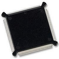
MC68332GCEH20 Freescale Semiconductor, MC68332GCEH20 Datasheet - Page 68

MC68332GCEH20
Manufacturer Part Number
MC68332GCEH20
Description
IC MCU 32BIT 20MHZ 132-PQFP
Manufacturer
Freescale Semiconductor
Series
M683xxr
Specifications of MC68332GCEH20
Core Processor
CPU32
Core Size
32-Bit
Speed
20MHz
Connectivity
EBI/EMI, SCI, SPI, UART/USART
Peripherals
POR, PWM, WDT
Number Of I /o
15
Program Memory Type
ROMless
Ram Size
2K x 8
Voltage - Supply (vcc/vdd)
4.5 V ~ 5.5 V
Oscillator Type
Internal
Operating Temperature
-40°C ~ 85°C
Package / Case
132-QFP
Controller Family/series
68K
No. Of I/o's
15
Ram Memory Size
2KB
Cpu Speed
20MHz
No. Of Timers
1
Embedded Interface Type
QSPI, SCI, UART
Digital Ic Case Style
PQFP
Rohs Compliant
Yes
Data Bus Width
32 bit
Data Ram Size
2 KB
Interface Type
QSPI, SCI, UART
Maximum Clock Frequency
20 MHz
Number Of Programmable I/os
15
Number Of Timers
16
Maximum Operating Temperature
+ 85 C
Mounting Style
SMD/SMT
Minimum Operating Temperature
- 40 C
Lead Free Status / RoHS Status
Lead free / RoHS Compliant
Eeprom Size
-
Program Memory Size
-
Data Converters
-
Lead Free Status / Rohs Status
Details
Available stocks
Company
Part Number
Manufacturer
Quantity
Price
Company:
Part Number:
MC68332GCEH20
Manufacturer:
Freescale Semiconductor
Quantity:
10 000
Part Number:
MC68332GCEH20
Manufacturer:
FREESCALE
Quantity:
20 000
QIVR — QSM Interrupt Vector Register
6.4.2 Pin Control Registers
PORTQS — Port QS Data Register
PQSPAR — PORT QS Pin Assignment Register
DDRQS — PORT QS Data Direction Register
68
MOTOROLA
RESET:
RESET:
15
15
15
0
0
At reset, QIVR is initialized to $0F, which corresponds to the uninitialized interrupt vector in the excep-
tion table. This vector is selected until QIVR is written. A user-defined vector ($40–$FF) should be writ-
ten to QIVR during QSM initialization.
After initialization, QIVR determines which two vectors in the exception vector table are to be used for
QSM interrupts. The QSPI and SCI submodules have separate interrupt vectors adjacent to each other.
Both submodules use the same interrupt vector with the least significant bit (LSB) determined by the
submodule causing the interrupt.
The value of INTV0 used during an interrupt-acknowledge cycle is supplied by the QSM. During an in-
terrupt-acknowledge cycle, INTV[7:1] are driven on DATA[7:1] IMB lines. DATA0 is negated for an SCI
interrupt and asserted for a QSPI interrupt. Writes to INTV0 have no meaning or effect. Reads of INTV0
return a value of one.
The QSM uses nine pins, eight of which form a parallel port (PORTQS) on the MCU. Although these
pins are used by the serial subsystems, any pin can alternately be assigned as general-purpose I/O on
a pin-by-pin basis.
Pins used for general-purpose I/O must not be assigned to the QSPI by register PQSPAR. To avoid
driving incorrect data, the first byte to be output must be written before DDRQS is configured. DDRQS
must then be written to determine the direction of data flow and to output the value contained in register
PORTQS. Subsequent data for output is written to PORTQS.
PORTQS latches I/O data. Writes drive pins defined as outputs. Reads return data present on the pins.
To avoid driving undefined data, first write a byte to PORTQS, then configure DDRQS.
Clearing a bit in the PQSPAR assigns the corresponding pin to general-purpose I/O; setting a bit as-
signs the pin to the QSPI. The PQSPAR does not affect operation of the SCI.
PQSPA6 PQSPA5 PQSPA4 PQSPA3
14
0
13
0
NOT USED
12
0
QILR
Freescale Semiconductor, Inc.
11
For More Information On This Product,
0
10
0
0
Go to: www.freescale.com
PQSPA1 PQSPA0
9
0
8
8
8
0
DDQS7 DDQS6 DDQS5 DDQS4 DDQS3 DDQS2 DDQS1 DDQS0
PQS7
7
0
7
0
7
0
RESET:
PQS6
0
6
0
6
0
PQS5
0
5
0
5
0
PQS4
0
4
0
4
0
INTV
PQS3
1
3
0
3
0
PQS2
1
2
0
2
0
MC68332TS/D
PQS1
1
$YFFC05
$YFFC14
1
0
$YFFC16
$YFFC17
1
0
MC68332
PQS0
0
1
0
0
0
0


