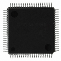
M38869FFAGP#U0 Renesas Electronics America, M38869FFAGP#U0 Datasheet - Page 8

M38869FFAGP#U0
Manufacturer Part Number
M38869FFAGP#U0
Description
IC 740/3886 MCU FLASH 80QFP
Manufacturer
Renesas Electronics America
Series
740/38000r
Datasheet
1.M38869FFAGPU0.pdf
(113 pages)
Specifications of M38869FFAGP#U0
Core Processor
740
Core Size
8-Bit
Speed
10MHz
Connectivity
I²C, SIO, UART/USART
Peripherals
PWM, WDT
Number Of I /o
64
Program Memory Size
60KB (60K x 8)
Program Memory Type
FLASH
Ram Size
2K x 8
Voltage - Supply (vcc/vdd)
4 V ~ 5.5 V
Data Converters
A/D 8x10b; D/A 2x8b
Oscillator Type
Internal
Operating Temperature
-20°C ~ 85°C
Package / Case
80-QFP
Lead Free Status / RoHS Status
Lead free / RoHS Compliant
Eeprom Size
-
Available stocks
Company
Part Number
Manufacturer
Quantity
Price
PIN DESCRIPTION
Table 1 Pin description (1)
V
V
AV
RESET
X
P3
P3
P3
CNV
X
P0
P1
P2
P0
CC
REF
IN
OUT
0
1
SS
2
0
0
0
1
Pin
/PWM
/PWM
–P3
/P3
–P1
–P2
, V
–P0
SS
SS
REF
7
7
7
7
00
10
Reference voltage
I/O port P1
I/O port P2
Power source
CNV
Analog power source
Reset input
Clock input
Clock output
I/O port P0
I/O port P3
SS
input
Name
•Apply voltage of 2.7 V – 5.5 V to Vcc, and 0 V to Vss.
•In the flash memory version, apply voltage of 4.0 V – 5.5 V to Vcc, and 0 V to Vss
•This pin controls the operation mode of the chip.
•Normally connected to V
•If this pin is connected to Vcc, the internal ROM is inhibited and an external memory is accessed.
•In the flash memory version, connected to V
•In the EPROM version or the flash memory version, this pin functions as the V
•Reference voltage input pin for A-D and D-A converters.
•Analog power source input pin for A-D and D-A converters.
•Connect to V
•Reset input pin for active “L”.
•Input and output pins for the clock generating circuit.
•Connect a ceramic resonator or quartz-crystal oscillator between the X
•When an external clock is used, connect the clock source to the X
•8-bit CMOS I/O port.
•I/O direction register allows each pin to be individually
•When the external memory is used, these pins are used as the address bus.
•CMOS compatible input level.
•CMOS 3-state output structure or N-channel open-drain output structure.
•8-bit CMOS I/O port.
•I/O direction register allows each pin to be individually programmed as either input or output.
•When the external memory is used, these pins are used as the address bus.
•CMOS compatible input level.
•CMOS 3-state output structure or N-channel open-drain output structure.
•8-bit CMOS I/O port.
•I/O direction register allows each pin to be individually programmed as either input or output.
•When the external memory is used, these pins are used as the data bus.
•CMOS compatible input level.
•CMOS 3-state output structure.
•P2
•8-bit CMOS I/O port.
•I/O direction register allows each pin to be individually
•When the external memory is used, these pins are
•CMOS compatible input level.
•CMOS 3-state output structure.
•These pins function as key-on wake-up and compara-
•These pins are enabled to control pull-up.
the oscillation frequency.
pin open.
programmed as either input or output.
programmed as either input or output.
used as the control bus.
tor input.
4
to P2
7
(4 bits) are enabled to output large current for LED drive (only in single-chip mode).
SS
.
Functions
SS
.
SINGLE-CHIP 8-BIT CMOS MICROCOMPUTER
SS.
MITSUBISHI MICROCOMPUTERS
•Comparator reference power source
input pin
•Key-on wake-up input pin
•Comparator input pin
•Key-on wake-up input pin
•Comparator input pin
•PWM output pin
Function except a port function
IN
PP
pin and leave the X
3886 Group
IN
power source input pin.
and X
OUT
pins to set
OUT
5


