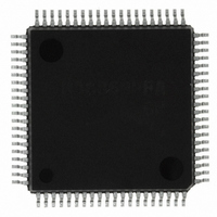
M38869FFAGP#U0 Renesas Electronics America, M38869FFAGP#U0 Datasheet - Page 38

M38869FFAGP#U0
Manufacturer Part Number
M38869FFAGP#U0
Description
IC 740/3886 MCU FLASH 80QFP
Manufacturer
Renesas Electronics America
Series
740/38000r
Datasheet
1.M38869FFAGPU0.pdf
(113 pages)
Specifications of M38869FFAGP#U0
Core Processor
740
Core Size
8-Bit
Speed
10MHz
Connectivity
I²C, SIO, UART/USART
Peripherals
PWM, WDT
Number Of I /o
64
Program Memory Size
60KB (60K x 8)
Program Memory Type
FLASH
Ram Size
2K x 8
Voltage - Supply (vcc/vdd)
4 V ~ 5.5 V
Data Converters
A/D 8x10b; D/A 2x8b
Oscillator Type
Internal
Operating Temperature
-20°C ~ 85°C
Package / Case
80-QFP
Lead Free Status / RoHS Status
Lead free / RoHS Compliant
Eeprom Size
-
Available stocks
Company
Part Number
Manufacturer
Quantity
Price
BUS INTERFACE
The 3886 group has a 2-byte bus interface function which is al-
most functionally equal to MELPS8-41 series and the control
signal from the host CPU side can operate it (slave mode).
It is possible to connect the 3886 group with the RD and WR
separated CPU bus directly. Figure 34 shows the block diagram of
the bus interface function.
The data bus buffer function I/O pins (P4
P5
0 (data bus buffer enable bit) of the data bus buffer control regis-
ter (address 002A
port I/O pins. When it is “1,” these bits become the data bus buffer
function I/O pins.
Fig. 32 Interrupt request circuit of data bus buffer
3
, P8) also function as the normal digital port I/O pins. When bit
O u t p u t b u f f e r
f u l l f l a g 0
O u t p u t b u f f e r
f u l l f l a g 1
I n p u t b u f f e r
f u l l f l a g 0
I n p u t b u f f e r
f u l l f l a g 1
(
O B F
O B E
(
O B E
O B F
I B F
I B F
I B F
O B E
16
) is “0,” these pins become the normal digital
O B F
O B F
0
I B F
I B F
0
1
0 )
1
1 )
0
1
0
1
O B E
O B E
R i s i n g e d g e
d e t e c t i o n c i r c u i t
R i s i n g e d g e
d e t e c t i o n c i r c u i t
0
1
2
, P4
R i s i n g e d g e
d e t e c t i o n c i r c u i t
R i s i n g e d g e
d e t e c t i o n c i r c u i t
3
, P4
6
, P4
7
, P5
O n e - s h o t p u l s e
g e n e r a t i n g c i r c u i t
O n e - s h o t p u l s e
g e n e r a t i n g c i r c u i t
0
I n t e r r u p t r e q u e s t i s s e t a t t h i s r i s i n g e d g e
–
O n e - s h o t p u l s e
g e n e r a t i n g c i r c u i t
O n e - s h o t p u l s e
g e n e r a t i n g c i r c u i t
I n t e r r u p t r e q u e s t i s s e t a t t h i s r i s i n g e d g e
The selection of either the single data bus buffer mode, which
uses 1 byte: data bus buffer 0 only, or the double data bus buffer
mode, which uses 2 bytes: data bus buffer 0 and data bus buffer
1, is performed by bit 1 (data bus buffer function selection bit) of
the data bus buffer control register (address 002A
comes S
written from the host CPU side, an input buffer full interrupt oc-
curs. When data is read from the host CPU, an output buffer
empty interrupt occurs. This microcomputer shares two input
buffer full interrupt requests and two output buffer empty interrupt
requests as shown in Figure 32, respectively.
1
input in the double data bus buffer mode. When data is
SINGLE-CHIP 8-BIT CMOS MICROCOMPUTER
MITSUBISHI MICROCOMPUTERS
I n p u t b u f f e r f u l l i n t e r r u p t
r e q u e s t s i g n a l I B F
O u t p u t b u f f e r e m p t y i n t e r r u p t
r e q u e s t s i g n a l O B E
3886 Group
16
). Port P4
7
be-
35


