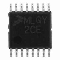
MCL908QY2CDTE Freescale Semiconductor, MCL908QY2CDTE Datasheet - Page 91

MCL908QY2CDTE
Manufacturer Part Number
MCL908QY2CDTE
Description
IC MCU 8BIT 1.5K FLASH 16-TSSOP
Manufacturer
Freescale Semiconductor
Series
HC08r
Datasheet
1.MCL908QY2CDWE.pdf
(182 pages)
Specifications of MCL908QY2CDTE
Core Processor
HC08
Core Size
8-Bit
Speed
2MHz
Peripherals
LVD, POR, PWM
Number Of I /o
13
Program Memory Size
1.5KB (1.5K x 8)
Program Memory Type
FLASH
Ram Size
128 x 8
Voltage - Supply (vcc/vdd)
2.4 V ~ 3.6 V
Data Converters
A/D 4x8b
Oscillator Type
Internal
Operating Temperature
-40°C ~ 85°C
Package / Case
16-TSSOP
Lead Free Status / RoHS Status
Lead free / RoHS Compliant
Eeprom Size
-
Connectivity
-
- Current page: 91 of 182
- Download datasheet (2Mb)
11.3.1.1 Internal Oscillator Trimming
The 8-bit trimming register, OSCTRIM, allows a clock period adjust of +127 and –128 steps. Increasing
OSCTRIM value increases the clock period. Trimming allows the internal clock frequency to be set to
4.0 MHz ±5%.
All devices are programmed with a trim value in a reserved FLASH location, $FFC0. This value can be
copied from the FLASH to the OSCTRIM register ($0038) during reset initialization.
Reset loads OSCTRIM with a default value of $80.
11.3.1.2 Internal to External Clock Switching
When external clock source (external OSC, RC, or XTAL) is desired, the user must perform the following
steps:
11.3.2 External Oscillator
The external clock option is designed for use when a clock signal is available in the application to provide
a clock source to the microcontroller. The OSC1 pin is enabled as an input by the oscillator module. The
clock signal is used directly to create BUSCLKX4 and also divided by two to create BUSCLKX2.
In this configuration, the OSC2 pin cannot output BUSCLKX4. So the OSC2EN bit in the port A pullup
enable register will be clear to enable PTA4 I/O functions on the pin.
Freescale Semiconductor
1. For external crystal circuits only, OSCOPT[1:0] = 1:1: To help precharge an external crystal
2. Set CONFIG2 bits OSCOPT[1:0] according to . The oscillator module control logic will then set
3. Create a software delay to wait the stabilization time needed for the selected clock source (crystal,
4. After the manufacturer’s recommended delay has elapsed, the ECGON bit in the OSC status
5. After ECGON set is detected, the OSC module checks for oscillator activity by waiting two external
6. The OSC module then switches to the external clock. Logic provides a glitch free transition.
7. The OSC module first sets the ECGST bit in the OSCSTAT register and then stops the internal
oscillator, set PTA4 (OSC2) as an output and drive high for several cycles. This may help the
crystal circuit start more robustly.
OSC1 as an external clock input and, if the external crystal option is selected, OSC2 will also be
set as the clock output.
resonator, RC) as recommended by the component manufacturer. A good rule of thumb for crystal
oscillators is to wait 4096 cycles of the crystal frequency, i.e., for a 4-MHz crystal, wait
approximately 1 msec.
register (OSCSTAT) needs to be set by the user software.
clock rising edges.
oscillator.
Bulk FLASH erasure will set location $FFC0 to $FF and the factory
programmed value will be lost.
Once transition to the external clock is done, the internal oscillator will only
be reactivated with reset. No post-switch clock monitor feature is
implemented (clock does not switch back to internal if external clock dies).
MC68HLC908QY/QT Family Data Sheet, Rev. 3
WARNING
NOTE
Functional Description
91
Related parts for MCL908QY2CDTE
Image
Part Number
Description
Manufacturer
Datasheet
Request
R
Part Number:
Description:
Manufacturer:
Freescale Semiconductor, Inc
Datasheet:
Part Number:
Description:
Manufacturer:
Freescale Semiconductor, Inc
Datasheet:
Part Number:
Description:
Manufacturer:
Freescale Semiconductor, Inc
Datasheet:
Part Number:
Description:
Manufacturer:
Freescale Semiconductor, Inc
Datasheet:
Part Number:
Description:
Manufacturer:
Freescale Semiconductor, Inc
Datasheet:
Part Number:
Description:
Manufacturer:
Freescale Semiconductor, Inc
Datasheet:
Part Number:
Description:
Manufacturer:
Freescale Semiconductor, Inc
Datasheet:
Part Number:
Description:
Manufacturer:
Freescale Semiconductor, Inc
Datasheet:
Part Number:
Description:
Manufacturer:
Freescale Semiconductor, Inc
Datasheet:
Part Number:
Description:
Manufacturer:
Freescale Semiconductor, Inc
Datasheet:
Part Number:
Description:
Manufacturer:
Freescale Semiconductor, Inc
Datasheet:
Part Number:
Description:
Manufacturer:
Freescale Semiconductor, Inc
Datasheet:
Part Number:
Description:
Manufacturer:
Freescale Semiconductor, Inc
Datasheet:
Part Number:
Description:
Manufacturer:
Freescale Semiconductor, Inc
Datasheet:
Part Number:
Description:
Manufacturer:
Freescale Semiconductor, Inc
Datasheet:


