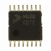
MC9S08QG84CDTE Freescale Semiconductor, MC9S08QG84CDTE Datasheet - Page 245

MC9S08QG84CDTE
Manufacturer Part Number
MC9S08QG84CDTE
Description
IC MCU 8BIT 8K FLASH 16-TSSOP
Manufacturer
Freescale Semiconductor
Series
HCS08r
Datasheet
1.MC9S08QG8CDTER.pdf
(314 pages)
Specifications of MC9S08QG84CDTE
Core Processor
HCS08
Core Size
8-Bit
Speed
20MHz
Connectivity
I²C, SCI, SPI
Peripherals
LVD, POR, PWM, WDT
Number Of I /o
12
Program Memory Size
8KB (8K x 8)
Program Memory Type
FLASH
Ram Size
512 x 8
Voltage - Supply (vcc/vdd)
1.8 V ~ 3.6 V
Data Converters
A/D 8x10b
Oscillator Type
Internal
Operating Temperature
-40°C ~ 85°C
Package / Case
16-TSSOP
Controller Family/series
HCS08
No. Of I/o's
12
Ram Memory Size
512Byte
Cpu Speed
20MHz
No. Of Timers
2
Embedded Interface Type
I2C, SCI, SPI
Rohs Compliant
Yes
For Use With
DEMO9S08QG8E - BOARD DEMO FOR MC9S08QG8
Lead Free Status / RoHS Status
Lead free / RoHS Compliant
Eeprom Size
-
Available stocks
Company
Part Number
Manufacturer
Quantity
Price
Company:
Part Number:
MC9S08QG84CDTE
Manufacturer:
Freescale Semiconductor
Quantity:
135
- Current page: 245 of 314
- Download datasheet (6Mb)
Chapter 17
Development Support
17.1
Introduction
Development support systems in the HCS08 include the background debug controller (BDC) and the
on-chip debug module (DBG). The BDC provides a single-wire debug interface to the target MCU that
provides a convenient interface for programming the on-chip FLASH and other nonvolatile memories. The
BDC is also the primary debug interface for development and allows non-intrusive access to memory data
and traditional debug features such as CPU register modify, breakpoints, and single instruction trace
commands.
In the HCS08 Family, address and data bus signals are not available on external pins. Debug is done
through commands fed into the target MCU via the single-wire background debug interface. The debug
module provides a means to selectively trigger and capture bus information so an external development
system can reconstruct what happened inside the MCU on a cycle-by-cycle basis without having external
access to the address and data signals.
17.1.1
Module Configuration
The alternate BDC clock source is the ICSLCLK. This clock source is selected by clearing the CLKSW
bit in the BDCSCR register. For details on ICSLCLK, see
Section 10.4, “Functional
Description” of the
ICS chapter.
MC9S08QG8 and MC9S08QG4 Data Sheet, Rev. 5
Freescale Semiconductor
243
Related parts for MC9S08QG84CDTE
Image
Part Number
Description
Manufacturer
Datasheet
Request
R
Part Number:
Description:
Hcs08 Microcontrollers
Manufacturer:
Freescale Semiconductor, Inc
Datasheet:
Part Number:
Description:
Manufacturer:
Freescale Semiconductor, Inc
Datasheet:
Part Number:
Description:
Manufacturer:
Freescale Semiconductor, Inc
Datasheet:
Part Number:
Description:
Manufacturer:
Freescale Semiconductor, Inc
Datasheet:
Part Number:
Description:
Manufacturer:
Freescale Semiconductor, Inc
Datasheet:
Part Number:
Description:
Manufacturer:
Freescale Semiconductor, Inc
Datasheet:
Part Number:
Description:
Manufacturer:
Freescale Semiconductor, Inc
Datasheet:
Part Number:
Description:
Manufacturer:
Freescale Semiconductor, Inc
Datasheet:
Part Number:
Description:
Manufacturer:
Freescale Semiconductor, Inc
Datasheet:
Part Number:
Description:
Manufacturer:
Freescale Semiconductor, Inc
Datasheet:
Part Number:
Description:
Manufacturer:
Freescale Semiconductor, Inc
Datasheet:
Part Number:
Description:
Manufacturer:
Freescale Semiconductor, Inc
Datasheet:
Part Number:
Description:
Manufacturer:
Freescale Semiconductor, Inc
Datasheet:
Part Number:
Description:
Manufacturer:
Freescale Semiconductor, Inc
Datasheet:
Part Number:
Description:
Manufacturer:
Freescale Semiconductor, Inc
Datasheet:


