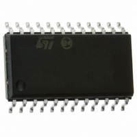
ST72F63BE2M1 STMicroelectronics, ST72F63BE2M1 Datasheet - Page 117

ST72F63BE2M1
Manufacturer Part Number
ST72F63BE2M1
Description
MCU 8BIT LS USB 8KB FLASH 24SOIC
Manufacturer
STMicroelectronics
Series
ST7r
Datasheet
1.ST72F63BD6U1TR.pdf
(186 pages)
Specifications of ST72F63BE2M1
Core Processor
ST7
Core Size
8-Bit
Speed
8MHz
Connectivity
I²C, SCI, USB
Peripherals
DMA, LVD, POR, PWM, WDT
Number Of I /o
14
Program Memory Size
8KB (8K x 8)
Program Memory Type
FLASH
Ram Size
1K x 8
Voltage - Supply (vcc/vdd)
4 V ~ 5.5 V
Oscillator Type
Internal
Operating Temperature
0°C ~ 70°C
Package / Case
24-SOIC (7.5mm Width)
Data Converters
A/D 12x10b
Processor Series
ST72F6x
Core
ST7
Data Bus Width
8 bit
Data Ram Size
384 B
Interface Type
I2C, SCI
Maximum Clock Frequency
8 MHz
Number Of Programmable I/os
14
Number Of Timers
1
Maximum Operating Temperature
+ 70 C
Mounting Style
SMD/SMT
Development Tools By Supplier
ST7MDTU3-EPB/US, ST7MDTULS-EVAL, ST72F63B-SK/RAIS, ST7MDTU3-EMU3, STX-RLINK
Minimum Operating Temperature
0 C
For Use With
497-8209 - BOARD EVAL USB STUSB02E/ST72F63B497-8208 - BOARD EVAL USB STUSB03E/ST72F63B497-5521 - EVAL BOARD LOW SPEED USB497-5046 - KIT TOOL FOR ST7/UPSD/STR7 MCU
Lead Free Status / RoHS Status
Lead free / RoHS Compliant
Eeprom Size
-
Lead Free Status / Rohs Status
Details
Other names
497-5624-5
Available stocks
Company
Part Number
Manufacturer
Quantity
Price
ST7263Bxx
11.5.7
Register description
I²C Control register (CR)
Reset value: 0000 0000 (00h)
7
0
[7:6] Reserved. Forced to 0 by hardware.
5 PE Peripheral enable.
4 ENGC Enable General Call.
3 START Generation of a Start condition. This bit is set and cleared by software. It is
This bit is set and cleared by software.
0: Peripheral disabled
1: Master/Slave capability
Note: When PE=0, all the bits of the CR register and the SR register except the
This bit is set and cleared by software. It is also cleared by hardware when the
interface is disabled (PE=0). The 00h General Call address is acknowledged (01h
ignored).
0: General Call disabled
1: General Call enabled
Note: In accordance with the I
also cleared by hardware when the interface is disabled (PE=0) or when the Start
condition is sent (with interrupt generation if ITE=1).
In master mode:
0: No start generation
1: Repeated start generation
In slave mode:
0: No start generation
1: Start generation when the bus is free
0
Stop bit are reset. All outputs are released while PE=0.
When PE=1, the corresponding I/O pins are selected by hardware as
alternate functions.
To enable the I²C interface, write the CR register TWICE with PE=1 as the
first write only activates the interface (only PE is set).
I
2
C slave can only receive data. It will not transmit data to the master.
PE
Doc ID 7516 Rev 8
ENGC
Read/write
2
C standard, when GCAL addressing is enabled, an
START
ACK
On-chip peripherals
STOP
117/186
ITE
0


