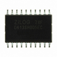
Z8F0413SH005EC Zilog, Z8F0413SH005EC Datasheet - Page 155

Z8F0413SH005EC
Manufacturer Part Number
Z8F0413SH005EC
Description
IC ENCORE MCU FLASH 4K 20SOIC
Manufacturer
Zilog
Series
Encore!® XP®r
Specifications of Z8F0413SH005EC
Core Processor
Z8
Core Size
8-Bit
Speed
5MHz
Connectivity
IrDA, UART/USART
Peripherals
Brown-out Detect/Reset, LED, POR, PWM, WDT
Number Of I /o
16
Program Memory Size
4KB (4K x 8)
Program Memory Type
FLASH
Ram Size
1K x 8
Voltage - Supply (vcc/vdd)
2.7 V ~ 3.6 V
Oscillator Type
Internal
Operating Temperature
-40°C ~ 105°C
Package / Case
20-SOIC (7.5mm Width)
Lead Free Status / RoHS Status
Contains lead / RoHS non-compliant
Eeprom Size
-
Data Converters
-
Other names
269-3486
- Current page: 155 of 247
- Download datasheet (4Mb)
Table 88. Flash Options Bits at Program Memory Address 0001H
BITS
FIELD
RESET
R/W
ADDR
Note: U = Unchanged by Reset. R/W = Read/Write.
PS024314-0308
Flash Program Memory Address 0001H
R/W
U
7
Watchdog Timer can only be disabled by a Reset or Stop Mode Recovery. This setting is
the default for unprogrammed (erased) Flash.
Reserved—R/W bits must be 1 during writes; 1 when read.
VBO_AO—Voltage Brownout Protection Always ON
0 = Voltage Brownout Protection can be disabled in STOP mode to reduce total power
consumption. For the block to be disabled, the power control register bit must also be writ-
ten (see
1 = Voltage Brownout Protection is always enabled including during STOP mode. This
setting is the default for unprogrammed (erased) Flash.
FRP—Flash Read Protect
0 = User program code is inaccessible. Limited control features are available through the
On-Chip Debugger.
1 = User program code is accessible. All On-Chip Debugger commands are enabled. This
setting is the default for unprogrammed (erased) Flash.
Reserved—Must be 1
FWP—Flash Write Protect
This Option Bit provides Flash Program Memory protection:
0 = Programming and erasure disabled for all of Flash Program Memory. Programming,
Page Erase, and Mass Erase through User Code is disabled. Mass Erase is available using
the On-Chip Debugger.
1 = Programming, Page Erase, and Mass Erase are enabled for all of Flash program
memory.
Reserved—R/W must be 1 during writes; 1 when read
XTLDIS—State of Crystal Oscillator at Reset
Reserved
Power Control Register 0
R/W
U
6
R/W
U
5
Program Memory 0001H
XTLDIS
R/W
on page 32).
U
4
R/W
U
3
Z8 Encore! XP
R/W
U
2
Reserved
Product Specification
R/W
U
1
®
Flash Option Bits
F0823 Series
R/W
U
0
145
Related parts for Z8F0413SH005EC
Image
Part Number
Description
Manufacturer
Datasheet
Request
R

Part Number:
Description:
Communication Controllers, ZILOG INTELLIGENT PERIPHERAL CONTROLLER (ZIP)
Manufacturer:
Zilog, Inc.
Datasheet:

Part Number:
Description:
KIT DEV FOR Z8 ENCORE 16K TO 64K
Manufacturer:
Zilog
Datasheet:

Part Number:
Description:
KIT DEV Z8 ENCORE XP 28-PIN
Manufacturer:
Zilog
Datasheet:

Part Number:
Description:
DEV KIT FOR Z8 ENCORE 8K/4K
Manufacturer:
Zilog
Datasheet:

Part Number:
Description:
KIT DEV Z8 ENCORE XP 28-PIN
Manufacturer:
Zilog
Datasheet:

Part Number:
Description:
DEV KIT FOR Z8 ENCORE 4K TO 8K
Manufacturer:
Zilog
Datasheet:

Part Number:
Description:
CMOS Z8 microcontroller. ROM 16 Kbytes, RAM 256 bytes, speed 16 MHz, 32 lines I/O, 3.0V to 5.5V
Manufacturer:
Zilog, Inc.
Datasheet:

Part Number:
Description:
Low-cost microcontroller. 512 bytes ROM, 61 bytes RAM, 8 MHz
Manufacturer:
Zilog, Inc.
Datasheet:

Part Number:
Description:
Z8 4K OTP Microcontroller
Manufacturer:
Zilog, Inc.
Datasheet:

Part Number:
Description:
CMOS SUPER8 ROMLESS MCU
Manufacturer:
Zilog, Inc.
Datasheet:

Part Number:
Description:
SL1866 CMOSZ8 OTP Microcontroller
Manufacturer:
Zilog, Inc.
Datasheet:

Part Number:
Description:
SL1866 CMOSZ8 OTP Microcontroller
Manufacturer:
Zilog, Inc.
Datasheet:

Part Number:
Description:
OTP (KB) = 1, RAM = 125, Speed = 12, I/O = 14, 8-bit Timers = 2, Comm Interfaces Other Features = Por, LV Protect, Voltage = 4.5-5.5V
Manufacturer:
Zilog, Inc.
Datasheet:

Part Number:
Description:
Manufacturer:
Zilog, Inc.
Datasheet:


