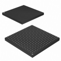
AT91SAM9M10-CU Atmel, AT91SAM9M10-CU Datasheet - Page 10

AT91SAM9M10-CU
Manufacturer Part Number
AT91SAM9M10-CU
Description
IC MCU 16/32BIT ARM9 324TFBGA
Manufacturer
Atmel
Series
AT91SAMr
Specifications of AT91SAM9M10-CU
Core Processor
ARM9
Core Size
16/32-Bit
Speed
400MHz
Connectivity
EBI/EMI, Ethernet, I²C, SPI, SSC, UART/USART, USB
Peripherals
AC'97, DMA, LCD, POR, PWM, WDT
Number Of I /o
160
Program Memory Size
64KB (64K x 8)
Program Memory Type
ROM
Ram Size
128K x 8
Voltage - Supply (vcc/vdd)
0.9 V ~ 1.1 V
Data Converters
A/D 8x10b
Oscillator Type
Internal
Operating Temperature
-40°C ~ 85°C
Package / Case
324-TFBGA
Processor Series
AT91SAMx
Core
ARM926EJ-S
Data Bus Width
32 bit
Data Ram Size
32 KB
Interface Type
2-Wire, SPI, USART
Maximum Clock Frequency
133 MHz
Number Of Programmable I/os
5
Number Of Timers
2 x 16 bit
Operating Supply Voltage
1.65 V to 3.6 V
Maximum Operating Temperature
+ 85 C
Mounting Style
SMD/SMT
3rd Party Development Tools
JTRACE-ARM-2M, MDK-ARM, RL-ARM, ULINK2
Development Tools By Supplier
AT91SAM-ICE, AT91-ISP, AT91SAM9M10-G45-EK
Controller Family/series
AT91
No. Of I/o's
160
Ram Memory Size
64KB
Cpu Speed
400MHz
No. Of Timers
2
Rohs Compliant
Yes
Cpu Family
AT91
Device Core
ARM926EJ-S
Device Core Size
32b
Frequency (max)
400MHz
Total Internal Ram Size
64KB
# I/os (max)
160
Number Of Timers - General Purpose
7
Operating Supply Voltage (typ)
1.8/2.5/3.3V
Operating Supply Voltage (max)
1.1/1.95/3.6V
Operating Supply Voltage (min)
0.9/1.65/1.8/3V
On-chip Adc
8-chx10-bit
Instruction Set Architecture
RISC
Operating Temp Range
-40C to 85C
Operating Temperature Classification
Industrial
Mounting
Surface Mount
Pin Count
324
Package Type
TFBGA
Lead Free Status / RoHS Status
Lead free / RoHS Compliant
Eeprom Size
-
Lead Free Status / Rohs Status
Lead free / RoHS Compliant
Available stocks
Company
Part Number
Manufacturer
Quantity
Price
Company:
Part Number:
AT91SAM9M10-CU
Manufacturer:
Atmel
Quantity:
996
Table 3-1.
Notes:
10
Signal Name
AD3Y
GPAD4-GPAD7
TSADTRG
TSADVREF
M
1. Refer to peripheral multiplexing tables in
2. When configured as an input, the NRST pin enables asynchronous reset of the device when asserted low. This allows con-
3. Programming of this pull-up resistor is performed independently for each I/O line through the PIO Controllers. After reset, all
AT91SAM9M10
nection of a simple push button on the NRST pin as a system-user reset.
the I/O lines default as inputs with pull-up resistors enabled, except those which are multiplexed with the External Bus Inter-
face signals that require to be enabled as Peripheral at reset. This is explicitly indicated in the column “Reset State” of the
peripheral multiplexing tables.
Signal Description List (Continued)
Analog input channel 3 or
Touch Screen Left channel
Analog Inputs
ADC Trigger
ADC Reference
Function
Section 9.4 “Peripheral Signals Multiplexing on I/O Lines”
Analog
Analog
Input
Analog
Type
Active
Level
Reference
VDDANA
VDDANA
VDDANA
VDDANA
Voltage
Comments
Multiplexed with AD3
for these signals.
6355BS–ATARM–21-Jun-10


