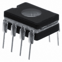
PIC12C671/JW Microchip Technology, PIC12C671/JW Datasheet - Page 579

PIC12C671/JW
Manufacturer Part Number
PIC12C671/JW
Description
IC MCU EPROM 1KX14 A/D 8CDIP
Manufacturer
Microchip Technology
Series
PIC® 12Cr
Datasheets
1.PIC16F688T-ISL.pdf
(688 pages)
2.PIC12CE673-10P.pdf
(129 pages)
3.PIC12CE673-10P.pdf
(14 pages)
Specifications of PIC12C671/JW
Core Processor
PIC
Core Size
8-Bit
Speed
10MHz
Peripherals
POR, WDT
Number Of I /o
5
Program Memory Size
1.75KB (1K x 14)
Program Memory Type
EPROM, UV
Ram Size
128 x 8
Voltage - Supply (vcc/vdd)
3 V ~ 5.5 V
Data Converters
A/D 4x8b
Oscillator Type
Internal
Operating Temperature
0°C ~ 70°C
Package / Case
8-CDIP (0.300", 7.62mm) Window
Lead Free Status / RoHS Status
Contains lead / RoHS non-compliant
Eeprom Size
-
Connectivity
-
Available stocks
Company
Part Number
Manufacturer
Quantity
Price
Part Number:
PIC12C671/JW
Manufacturer:
MICROCH
Quantity:
20 000
- Current page: 579 of 688
- Download datasheet (3Mb)
30.6
DC CHARACTERISTICS
D030
D030A
D031
D032
D033
D040
D040A
D041
D042
D042A
D043
D050
Note 1: In RC oscillator configuration, the OSC1/CLKIN pin is a Schmitt Trigger input. It is not recommended that the
Param
1997 Microchip Technology Inc.
No.
† Data in “Typ” column is at 5V, 25 C unless otherwise stated. These parameters are for design guidance only
2: Not Applicable.
3: Not Applicable.
4: The better of the two specifications may be used. For V
and are not tested.
PICmicro be driven with an external clock while in RC mode.
would be the lower voltage.
Symbol
V
Input Threshold Levels
V
V
HYS
IH
IL
Input Low Voltage
I/O ports:
MCLR, OSC1 (RC mode)
OSC1
(XT, HS and LP modes)
Input High Voltage
MCLR
OSC1
(XT, HS and LP modes)
OSC1 (RC mode)
Hysteresis of Schmitt Trigger
Inputs
with Schmitt Trigger buffer
with TTL buffer
with Schmitt Trigger buffer
I/O ports:
with TTL buffer
The Input Low Voltage (V
read a ’0’ at a voltage level above this. All designs should be to the specification since device to
device (and to a much lesser extent pin to pin) variations will cause this level to vary.
The Input High Voltage (V
read a ’1’ at a voltage level below this. All designs should be to the specification since device to
device (and to a much lesser extent pin to pin) variations will cause this level to vary.
The I/O pins with TTL levels are shown with two specifications. One is the industry standard TTL
specification, which is specified for the voltage range of 4.5V to 5.5V. The other is a specification
that operates over the entire voltage range of the device. The better of these two specifications
may be used in the design.
Table 30-6:
Section 30. Electrical Specifications
Characteristic
Example DC Characteristics
(1)
(1)
IL
Standard Operating Conditions (unless otherwise stated)
Operating temperature
Operating voltage V
IH
) is the voltage level that will be read as a logic ’0’. An input may not
0.25V
) is the voltage level that will be read as a logic ’1’. An input may
0.8V
0.7V
0.8V
0.9V
+ 0.8V
TBD
Min
V
V
V
V
2.0
—
SS
SS
SS
SS
DD
DD
DD
DD
DD
Typ†
—
—
—
—
—
—
—
—
—
—
—
—
IL
this would be the higher voltage and for V
DD
0.15V
0.2V
0.2V
0.3V
Max
V
V
V
V
V
V
0.8
range as described in DC spec
—
DD
DD
DD
DD
DD
DD
DD
DD
DD
0˚C
-40˚C
-40˚C
DD
Units
V
V
V
V
V
V
V
V
V
V
V
V
T
T
T
A
A
A
For entire V
4.5V
For entire V
For entire V
4.5V
For entire V
+70˚C for commercial,
+85˚C for industrial and
+125˚C for extended
V
V
Conditions
DD
DD
DS31030A-page 30-9
DD
DD
DD
DD
5.5V
5.5V
range
range
range
range
Table
(4)
(4)
IH
(4)
(4)
30-3.
this
30
Related parts for PIC12C671/JW
Image
Part Number
Description
Manufacturer
Datasheet
Request
R

Part Number:
Description:
8-Pin/ 8-Bit CMOS Microcontroller with EEPROM Data Memory
Manufacturer:
Microchip Technology

Part Number:
Description:
IC, 8BIT MCU, PIC12, 32MHZ, DFN-8
Manufacturer:
Microchip Technology
Datasheet:

Part Number:
Description:
IC, 8BIT MCU, PIC12, 32MHZ, DFN-8
Manufacturer:
Microchip Technology
Datasheet:

Part Number:
Description:
Manufacturer:
Microchip Technology Inc.
Datasheet:

Part Number:
Description:
Manufacturer:
Microchip Technology Inc.
Datasheet:

Part Number:
Description:
Manufacturer:
Microchip Technology Inc.
Datasheet:

Part Number:
Description:
Manufacturer:
Microchip Technology Inc.
Datasheet:

Part Number:
Description:
Manufacturer:
Microchip Technology Inc.
Datasheet:

Part Number:
Description:
Manufacturer:
Microchip Technology Inc.
Datasheet:

Part Number:
Description:
Manufacturer:
Microchip Technology Inc.
Datasheet:


