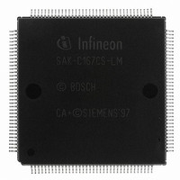
SAK-C167CS-LM CA+ Infineon Technologies, SAK-C167CS-LM CA+ Datasheet - Page 65

SAK-C167CS-LM CA+
Manufacturer Part Number
SAK-C167CS-LM CA+
Description
IC MCU 16BIT 25MHZ MQFP-144
Manufacturer
Infineon Technologies
Series
C16xxr
Datasheet
1.SAK-C167CS-LM_CA.pdf
(81 pages)
Specifications of SAK-C167CS-LM CA+
Core Processor
C166
Core Size
16-Bit
Speed
25MHz
Connectivity
CAN, EBI/EMI, SPI, SSC, UART/USART
Peripherals
POR, PWM, WDT
Number Of I /o
111
Program Memory Type
ROMless
Ram Size
11K x 8
Voltage - Supply (vcc/vdd)
4.5 V ~ 5.5 V
Data Converters
A/D 24x10b
Oscillator Type
External
Operating Temperature
-40°C ~ 125°C
Package / Case
144- BSQFP
Packages
PG-MQFP-144
Max Clock Frequency
25.0 MHz
Sram (incl. Cache)
11.0 KByte
Can Nodes
2
A / D Input Lines (incl. Fadc)
24
Program Memory
0.0 KByte
Lead Free Status / RoHS Status
Lead free / RoHS Compliant
Eeprom Size
-
Program Memory Size
-
Other names
K167CSLMCAZNP
K167CSLMCAZXP
K167CSLMCAZXT
SAK-C167CS-LM CA+
SAK-C167CS-LMCAIN
SAKC167CSLMCAT
SP000103492
K167CSLMCAZXP
K167CSLMCAZXT
SAK-C167CS-LM CA+
SAK-C167CS-LMCAIN
SAKC167CSLMCAT
SP000103492
5)
6)
7)
8)
Sample time and conversion time of the C167CS’s A/D Converter are programmable.
Table 14
The limit values for
Table 14
ADCON.15|14
(ADCTC)
00
01
10
11
Converter Timing Example:
Assumptions:
Basic clock
Sample time
Conversion time
Data Sheet
As the default basic clock after reset is
a valid factor as early as possible. A timeframe of approx. 6000 CPU clock cycles is sufficient to ensure a
proper reset calibration. This corresponds to minimum 300 instructions (worst case: external MUX bus with
maximum waitstates). This is required for
During the reset calibration conversions can be executed (with the current accuracy). The time required for
these conversions is added to the total reset calibration time.
During the conversion the ADC’s capacitance must be repeatedly charged or discharged. The internal
resistance of the reference voltage source must allow the capacitance to reach its respective voltage level
within each conversion step. The maximum internal resistance results from the programmed conversion
timing.
Not 100% tested, guaranteed by design and characterization.
During the sample time the input capacitance
internal resistance of the analog source must allow the capacitance to reach its final voltage level within
After the end of the sample time
Values for the sample time
should be used to calculate the above timings.
A/D Converter Computation Table
A/D Converter
Basic Clock
f
f
f
f
CPU
CPU
CPU
CPU
f
f
t
t
f
CPU
BC
S
C
BC
/ 4
/ 2
/ 16
/ 8
must not be exceeded when selecting ADCTC.
t
S
depend on programming and can be taken from
= 25 MHz (i.e.
=
=
=
t
S
f
t
t
, changes of the analog input voltage have no effect on the conversion result.
CPU
BC
S
f
+ 40
BC
× 8 = 1280 ns.
f
/ 4 = 6.25 MHz, i.e.
BC
t
f
=
BC
CPU
f
CPU
C
+ 2
> 33 MHz and is recommended for
AIN
t
CPU
/ 4 the ADC’s prescaler (ADCTC) must be programmed to
61
can be charged/discharged by the external source. The
t
CPU
ADCON.13|12
(ADSTC)
00
01
10
11
= 40 ns), ADCTC = ‘00’, ADSTC = ‘00’.
= (1280 + 6400 + 80) ns = 7.8 µ s.
t
BC
= 160 ns.
Sample time
t
t
t
t
t
S
BC
BC
BC
BC
Table
× 8
× 16
× 32
× 64
f
CPU
14.
> 25 MHz.
C167CS-4R
V2.2, 2001-08
C167CS-L
t
S
.


