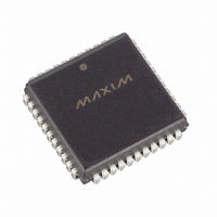
DS80C320-QCG+ Maxim Integrated Products, DS80C320-QCG+ Datasheet - Page 11

DS80C320-QCG+
Manufacturer Part Number
DS80C320-QCG+
Description
IC MCU HI SPEED 25MHZ 44-PLCC
Manufacturer
Maxim Integrated Products
Series
80Cr
Datasheet
1.DS80C323-QND.pdf
(38 pages)
Specifications of DS80C320-QCG+
Core Processor
8051
Core Size
8-Bit
Speed
25MHz
Connectivity
EBI/EMI, SIO, UART/USART
Peripherals
Power-Fail Reset, WDT
Number Of I /o
32
Program Memory Type
ROMless
Ram Size
256 x 8
Voltage - Supply (vcc/vdd)
4.5 V ~ 5.5 V
Oscillator Type
External
Operating Temperature
0°C ~ 70°C
Package / Case
44-LCC, 44-PLCC
Controller Family/series
(8051) 8052
No. Of I/o's
32
Ram Memory Size
256Byte
Cpu Speed
25MHz
No. Of Timers
3
Embedded Interface Type
UART
Digital Ic Case Style
LCC
Rohs Compliant
Yes
Processor Series
DS80C320
Core
8051
Data Bus Width
8 bit
Program Memory Size
64 KB
Data Ram Size
64 KB
Interface Type
UART
Maximum Clock Frequency
25 MHz
Number Of Programmable I/os
32
Number Of Timers
3
Operating Supply Voltage
4.25 V to 5.5 V
Maximum Operating Temperature
+ 70 C
Mounting Style
SMD/SMT
3rd Party Development Tools
PK51, CA51, A51, ULINK2
Minimum Operating Temperature
0 C
For Use With
MCBX51 - BOARD EVALUATION 8051/251 44PIN
Lead Free Status / RoHS Status
Lead free / RoHS Compliant
Eeprom Size
-
Program Memory Size
-
Data Converters
-
Lead Free Status / Rohs Status
Details
Table 1 shows the speed for each class of instruction. Note that many of the instructions have multiple op
codes. There are 255 op codes for 111 instructions. Of the 255 op codes, 159 are three times faster than
the original 80C32. While a system that emphasizes those instructions will see the most improvement, the
large total number that receive a 3 to 1 improvement assure a dramatic speed increase for any system. The
speed improvement summary is provided below.
SPEED ADVANTAGE SUMMARY
MEMORY ACCESS
The DS80C320/DS80C323 do not contain on-chip ROM and 256 bytes of scratchpad RAM. Off-chip
memory is accessed using the multiplexed address/data bus on P0 and the MSB address on P2. Figure 3
shows a typical memory connection. Timing diagrams are provided in the Electrical Specifications
section. Program memory (ROM) is accessed at a fixed rate determined by the crystal frequency and the
actual instructions. As previously mentioned, an instruction cycle requires 4 clocks. Data memory (RAM)
is accessed according to a variable-speed MOVX instruction as described below.
Figure 3. Typical Memory Connection
#OP CODES
255
159
51
43
2
IMPROVEMENT
Average: 2.5
SPEED
3.0 x
1.5 x
2.0 x
2.4 x
DS80C320/DS80C323 High-Speed/Low-Power Microcontrollers
11 of 38


