SAB-C505CA-4EM CA Infineon Technologies, SAB-C505CA-4EM CA Datasheet
SAB-C505CA-4EM CA
Specifications of SAB-C505CA-4EM CA
B505CA4EMCAXP
SAB-C505CA-4EMCA
SAB-C505CA-4EMCA
SAB-C505CA-4EMCAIN
SABC505CA4EMCAX
SP000106391


Related parts for SAB-C505CA-4EM CA


SAB-C505CA-4EM CA Summary of contents
Page 1
...
Page 2
... Infineon Technologies Office. Infineon Technologies Components may only be used in life-support devices or systems with the express written approval of Infineon Technologies failure of such components can reasonably be expected to cause the failure of that life-support device or system affect the safety or effectiveness of that device or system. Life support devices or systems are intended to be implanted in the human body support and/or maintain and sustain and/or protect human life ...
Page 3
...
Page 4
C505/C505C/C505A/C505CA Data Sheet Revision History : Previous Releases : Page Page Subjects (major changes since last revision) (in previous (in current version version Version register VR2 for C505A-4R/C505CA-4R BB step is updated. Controller Area Network (CAN): License of ...
Page 5
Single-Chip Microcontroller C500 Family Advance Information • Fully compatible to standard 8051 microcontroller • Superset of the 8051 architecture with 8 datapointers • MHz operating frequency – 375 ns instruction cycle time @16 MHz – 300 ...
Page 6
... Idle mode (can be combined with slow-down mode) – Software power-down mode with wake up capability through P3.2/INT0 or P4.1/RXDC pin • P-MQFP-44 package • Pin configuration is compatible to C501, C504, C511/C513-family • Temperature ranges: SAB-C505 versions SAF-C505 versions SAH-C505 versions SAK-C505 versions Data Sheet C505/C505C/C505A/C505CA TM ) ...
Page 7
... Note: The term C505(C)(A)-2R, for simplicity, is used to stand for C505 16K byte ROM versions within this document which are C505-2R, C505C-2R, C505A-2R and C505CA-2R. Ordering Information The ordering code for Infineon Technologies’ microcontrollers provides an exact reference to the required product. This ordering code identifies: • ...
Page 8
V AREF V AGND XTAL1 XTAL2 RESET EA ALE PSEN Figure 2 Logic Symbol Note: The ordering codes for the Mask-ROM versions are defined for each product after verification of the respective ROM code. Data Sheet C505/C505C/C505A/C505CA ...
Page 9
P0.3 / AD3 P0.2 / AD2 P0.1 / AD1 P0.0 / AD0 V AREF V AGND P1.0 / AN0 / INT3 / CC0 P1.1 / AN1 / INT4 / CC1 P1.2 / AN2 / INT5 / CC2 P1.3 / AN3 ...
Page 10
Table 2 Pin Definitions and Functions Symbol Pin Number P1.0-P1.7 40-44,1 Input O = Output Data Sheet I/O Function *) I/O Port 8-bit quasi-bidirectional port with ...
Page 11
Table 2 Pin Definitions and Functions (cont’d) Symbol Pin Number RESET 4 P3.0-P3 Input O = Output Data Sheet I/O Function *) I RESET A high level ...
Page 12
Table 2 Pin Definitions and Functions (cont’d) Symbol Pin Number P4.0 6 P4.1 28 XTAL2 14 XTAL1 Input O = Output Data Sheet I/O Function *) I/O Port 4 I 2-bit quasi-bidirectional port with ...
Page 13
... It is activated every three oscillator periods except during an external data memory access. When instructions are executed from internal ROM or OTP (EA=1) the ALE generation can be disabled by bit EALE in SFR SYSCON. ALE should not be driven during reset operation. 9 C505/C505C/C505A/C505CA ...
Page 14
Table 2 Pin Definitions and Functions (cont’d) Symbol Pin Number EA 29 P0.0-P0.7 37- AREF 39 V AGND Input O = Output Data Sheet I/O Function *) I External ...
Page 15
V DD Oscillator Watchdog Vss XTAL1 OSC & Timing XTAL2 CPU RESET 8 datapointers ALE PSEN Programmable EA Watchdog Timer Timer 0 Timer 1 Timer 2 USART Baudrate generator Full-CAN Controller Interrupt Unit V AREF A/D Converter 8-/10-Bit V AGND ...
Page 16
CPU The C505 is efficient both as a controller and as an arithmetic processor. It has extensive facilities for binary and BCD arithmetic and excels in its bit-handling capabilities. Efficient use of program memory results from an instruction set consisting ...
Page 17
Memory Organization The C505 CPU manipulates operands in the following four address spaces: – On-chip program memory :16K byte ROM (C505(C)(A)-2R) or – Totally up to 64K byte internal/external program memory – Kbyte of external data memory ...
Page 18
Reset and System Clock The reset input is an active high input at pin RESET. Since the reset is synchronized internally, the RESET pin must be held high for at least two machine cycles (12 oscillator periods) while the oscillator ...
Page 19
Figure 7 shows the recommended oscillator circuits for crystal and external clock operation. External Clock Signal Figure 7 Recommended Oscillator Circuitries Data Sheet C XTAL2 C505C 2-20 C505A MHz C505CA C XTAL1 C = 20pF ± 10pF for crystal operation ...
Page 20
Multiple Datapointers As a functional enhancement to the standard 8051 architecture, the C505 contains eight 16-bit datapointers instead of only one datapointer. The instruction set uses just one of these datapointers at a time. The selection of the actual datapointer ...
Page 21
Enhanced Hooks Emulation Concept The Enhanced Hooks Emulation Concept of the C500 microcontroller family is a new, innovative way to control the execution of C500 MCUs and to gain extensive information on the internal operation of the controllers. Emulation of ...
Page 22
... RMAP must be cleared/set respectively by software. All SFRs with addresses where address bits 0-2 are 0 (e. ..., are bitaddressable. The 52 special function registers (SFRs) in the standard and mapped SFR area include pointers and registers that provide an interface between the CPU and the other on-chip peripherals. The SFRs of the C505 are listed in refer to the functional blocks of the C505 ...
Page 23
... SYSCON 2) System Control Register 1) Bit-addressable special function registers 2) This special function register is listed repeatedly since some bits of it also belong to other functional blocks. 3) “X“ means that the value is undefined and the location is reserved 4) This SFR is a mapped SFR. For accessing this SFR, bit RMAP in SFR SYSCON must be set. ...
Page 24
... Modes PCON1 Power Control Register 1 1) Bit-addressable special function registers 2) This special function register is listed repeatedly since some bits of it also belong to other functional blocks. 3) “X“ means that the value is undefined and the location is reserved 4) SFR is located in the mapped SFR area. For accessing this SFR, bit RMAP in SFR SYSCON must be set. ...
Page 25
... DB7 Message Data Byte 7 1) Bit-addressable special function registers 2) This special function register is listed repeatedly since some bits of it also belong to other functional blocks. 3) “X“ means that the value is undefined and the location is reserved. “U“ means that the value is unchanged by a reset operation. “ ...
Page 26
... H SCON SBUF IEN0 IP0 SRELL means that the value is undefined and the location is reserved 2) Bit-addressable special function registers 3) SFR is located in the mapped SFR area. For accessing this SFR, bit RMAP in SFR SYSCON must be set. Data Sheet Bit 7 Bit 6 Bit 5 Bit ...
Page 27
... CB H CRCH TL2 TH2 PSW ADCON0 00X0- 0000 means that the value is undefined and the location is reserved 2) Bit-addressable special function registers 3) C505 /C505C/C505A only 4) C505CA only Data Sheet Bit 7 Bit 6 Bit 5 Bit – – EALE RMAP CMOD – – – EALE ...
Page 28
... H 10 means that the value is undefined and the location is reserved 2) Bit-addressable special function registers 3) SFR is located in the mapped SFR area. For accessing this SFR, bit RMAP in SFR SYSCON must be set. 4) These are read-only registers 5) The content of this SFR varies with the actual of the step C505 (eg. 01 ...
Page 29
Table 5 Contents of the CAN Registers in numeric order of their addresses (C505C/C505CA only) Addr. Register Content n=1-F H after 2) 1) Reset F700 F701 F702 F704 ...
Page 30
Table 5 Contents of the CAN Registers in numeric order of their addresses (cont’d) (C505C/C505CA only) Addr. Register Content n=1-F H after 2) 1) Reset F7n6 H MCFG UUUU. UU00 B F7n7 H DB0 XX H F7n8 H DB1 XX ...
Page 31
... The 8 analog inputs, AN0-AN7, are located at the port 1 pins P1.0 to P1.7. After reset, all analog inputs are disabled and the related pins of port 1 are configured as digital inputs. The analog function of a specific port 1 pin is enabled by bits in the SFR P1ANA ...
Page 32
Timer / Counter 0 and 1 Timer/Counter 0 and 1 can be used in four operating modes as listed in Table 6 Timer/Counter 0 and 1 Operating Modes Mode Description 0 8-bit timer/counter with a divide-by-32 prescaler 1 16-bit timer/counter ...
Page 33
Timer/Counter 2 with Compare/Capture/Reload The timer 2 of the C505 provides additional compare/capture/reload features. which allow the selection of the following operating modes: – Compare : PWM signals with 16-bit/300 ns resolution (@ 20 MHz clock) – ...
Page 34
Timer 2 Operating Modes The timer 2, which is a 16-bit-wide register, can operate as timer, event counter, or gated timer. A roll-over of the count value in TL2/TH2 from all 1’s to all 0’s sets the timer overflow flag ...
Page 35
Timer 2 Compare Modes The compare function of a timer/register combination operates as follows : the 16-bit value stored in a compare or compare/capture register is compared with the contents of the timer register; if the count value in the ...
Page 36
Compare Mode 1 If compare mode 1 is enabled and the software writes to the appropriate output latch at the port, the new value will not appear at the output pin until the next compare match occurs. Thus, it can ...
Page 37
Serial Interface (USART) The serial port is full duplex and can operate in four modes (one synchronous mode, three asynchronous modes) as illustrated in Table 7 USART Operating Modes SCON Mode SM0 SM1 ...
Page 38
Timer 1 Overflow Baud Rate Generator f OSC (SRELH SRELL) ÷ 6 Note: The switch configuration shows the reset state. Figure 14 Block Diagram of Baud Rate Generation for the Serial Interface Table 8 below lists the values/formulas for the ...
Page 39
CAN Controller (C505C and C505CA only) The on-chip CAN controller, compliant to version 2.0B, is the functional heart which provides all resources that are required to run the standard CAN protocol (11-bit identifiers) as well as the extended CAN protocol ...
Page 40
Messages Handlers Status + Control to internal Bus Figure 15 CAN Controller Block Diagram Data Sheet TXDC BTL-Configuration CRC Gen./Check TX/RX Shift Register Messages Intelligent Memory Interrupt Register Bit Stream Processor Status Register 36 C505/C505C/C505A/C505CA RXDC Bit Timing Logic Timing ...
Page 41
... Condition: CMOD = 0, when Frequency (MHz) f OSC Note : The switch configuration shows the reset state of bit CMOD. Figure 16 CAN controller Input Clock Selection Data Sheet (Figure 16). Setting bit CMOD (SYSCON.3) disables the SYSCON.3 (CMOD CAN 0 f > 10 MHz OSC CMOD BRP (SYSCON.3) (BTR0 ...
Page 42
A/D Converter (C505 and C505C only) The C505/C505C includes a high performance / high speed 8-bit A/D converter (ADC) with 8 analog input channels. It operates with a successive approximation technique and provides the following features: – 8 multiplexed ...
Page 43
IEN1 ( EXEN2 SWDT IRCON ( EXF2 TF2 P1ANA ( EAN7 EAN6 ADCON1 ( ADCL1 ADCL0 ADCON0 ( CLK Port 1 MUX Conversion f OSC Clock Prescaler V AREF ...
Page 44
A/D Converter (C505A and C505CA only) The C505A/C505CA includes a high performance / high speed 10-bit A/D-Converter (ADC) with 8 analog input channels. It operates with a successive approximation technique and uses self calibration mechanisms for reduction and compensation ...
Page 45
IEN1 ( EXEN2 SWDT IRCON ( EXF2 TF2 P1ANA ( EAN7 EAN6 ADCON1 ( ADCL1 ADCL0 ADCON0 ( CLK Port 1 MUX Conversion f OSC Clock Prescaler V AREF ...
Page 46
Interrupt System The C505 provides 12 interrupt vectors with four priority levels. Five interrupt requests can be generated by the on-chip peripherals (timer 0, timer 1, timer 2, serial interface, A/D converter). One interrupt can be generated by the CAN ...
Page 47
... CR.3 Message Transmit >1 TXIE MCR0 Message Receive RXIE MCR0 Bit addressable Request flag is cleared by hardware Figure 21 Interrupt Structure, Overview Part 1 Note: Each of the 15 CAN controller message objects (C505C and C505CA only), shown in the shaded area of Figure 21 Data Sheet IE0 0003 ...
Page 48
... P3.3 / INT1 IT1 TCON.2 P1.0 / AN0 / INT3 / CC0 I3FR T2CON.6 Timer 1 Overflow P1.1 / AN1 / INT4 / CC1 Bit addressable Request flag is cleared by hardware Figure 22 Interrupt Structure, Overview Part 2 Data Sheet IE1 0013 H TCON.3 EX1 IEN0.2 IEX3 0053 H IRCON.2 EX3 IEN1.2 IP1.2 TF1 ...
Page 49
... AN2 / INT5 / CC2 Timer 2 TF2 Overflow IRCON.6 P1.5 / AN5 / EXF2 T2EX IRCON.7 EXEN2 IEN1.7 P1.3 / INT6 / CC3 Bit addressable Request flag is cleared by hardware Figure 23 Interrupt Structure, Overview Part 3 Data Sheet >1 0023 H ES IEN0.4 IEX5 0063 H IRCON.4 EX5 IEN1.4 IP1.4 >1 ...
Page 50
Fail Save Mechanisms The C505 offers enhanced fail safe mechanisms, which allow an automatic recovery from software upset or hardware failure : – a programmable watchdog timer (WDT), with variable time-out period from 192 approx. 393.2 ms ...
Page 51
Oscillator Watchdog The oscillator watchdog unit serves for three functions: – Monitoring of the on-chip oscillator's function The watchdog supervises the on-chip oscillator's frequency lower than the frequency of the auxiliary RC oscillator in the watchdog unit, ...
Page 52
EWPD WS (PCON1.7) (PCON1.4) P4.1 / RXDC Control P3.2 / INT0 Logic Start / Stop RC f Oscillator RC 3 MHz Start / XTAL1 Stop On-Chip XTAL2 Oscillator Figure 25 Functional Block Diagram of the Oscillator Watchdog Data Sheet C505/C505C/C505A/C505CA ...
Page 53
Power Saving Modes The C505 provides two basic power saving modes, the idle mode and the power down mode. Additionally, a slow down mode is available. This power saving mode reduces the internal clock rate in normal operating mode and ...
Page 54
OTP Memory Operation (C505A-4E and C505CA-4E only) The C505A-4E/C505CA-4E contains a 32K byte one-time programmable (OTP) program memory. With the C505A-4E/C505CA-4E fast programming cycles are achieved (1 byte in 100 sec). Also several levels of OTP memory protection can be ...
Page 55
Pin Configuration in Programming Mode N.C. N.C. N.C. N.C. N.C. N.C. N.C. Figure 27 P-MQFP-44 Pin Configuration of the C505A-4E/C505CA-4E in Programming Mode (Top View) Data Sheet ...
Page 56
The following Table 11 contains the functional description of all C505A-4E/C505CA-4E pins which are required for OTP memory programming. Table 11 Pin Definitions and Functions in Programming Mode Symbol Pin Number I/O *) RESET 4 I PMSEL0 5 I PMSEL1 ...
Page 57
Table 11 Pin Definitions and Functions in Programming Mode (cont’d) Symbol Pin Number I/O *) P2.0-7 18-25 I PSEN 26 I PROG 27 I EA/V 29 – PP D7-0 30-37 I/O N.C. 1-3, 6, 11-13, – 28, 38- ...
Page 58
Basic Programming Mode Selection The basic programming mode selection scheme is shown Clock (XTAL1/XTAL2) RESET PSEN PMSEL1,0 PROG PRD PSEL PALE EA/V PP Figure 28 Basic Programming Mode Selection Data Sheet stable “1“ 0,1 “0“ “0“ 0V ...
Page 59
... Protection Type The OTP lock feature is disabled. During normal operation of the C505A-4E/C505CA-4E, the state of the EA pin is not latched on reset. During normal operation of the C505A-4E/C505CA-4E, MOVC instructions executed from external program memory are disabled from fetching code bytes from internal memory sampled and latched on reset. An OTP memory read operation is only possible using the ROM/OTP verification mode 2 for protection level 1 ...
Page 60
Absolute Maximum Ratings Parameter Storage temperature Voltage on V pins with respect ground ( ) SS Voltage on any pin with respect V to ground ( ) SS Input current on any pin during overload condition Absolute ...
Page 61
... Operating Conditions Parameter Symbol Supply voltage V DD Ground voltage V SS Ambient temperature SAB-C505 T A SAF-C505 T A SAH-C505 T A SAK-C505 Analog reference AREF voltage V Analog ground voltage AGND V Analog input voltage AIN XTAL clock f osc 1) For the extended temperature range -40 °C to 110 °C (SAH) and -40 °C to 125 °C (SAK), the devices C505-2R, C505-L, C505C-2R and C505C-L have the max ...
Page 62
DC Characteristics (Operating Conditions apply) Parameter Input low voltages all except EA, RESET EA pin RESET pin Input high voltages all except XTAL1, RESET XTAL1 pin RESET pin Output low voltages Ports Port 0, ALE, PSEN ...
Page 63
Power Supply Currents Parameter C505 / Active Mode C505C Idle Mode Active Mode with slow-down enabled Idle Mode with slow-down enabled Power down mode C505A-4E Active Mode /C505CA-4E Idle Mode Active Mode with slow-down enabled Idle Mode with slow-down enabled ...
Page 64
... I 7) (active mode) is measured with XTAL1 driven with , ns, 50% duty cycle , Port 0 = RESET = (idle mode) is measured with all output pins disconnected and with all peripherals disabled XTAL1 driven with , ns, 50% duty cycle RESET = Port0 = SS software (active mode with slow-down mode) is measured with all output pins disconnected and with all peripherals DD disabled ...
Page 65
I DD [mA Figure 29 I Diagram of C505 and C505C DD C505/C505C : Power Supply Current Calculation Formulas Parameter Symbol I Active mode DD typ I DD max I Idle ...
Page 66
I DD [mA Figure 30 I Diagram of C505A-4E and C505CA-4E DD C505A-4E/C505CA-4E : Power Supply Current Calculation Formulas Parameter Symbol Active mode I DD typ I DD max I Idle ...
Page 67
I DD [mA Figure 31 I Diagram of C505A-4R/C505A-2R/C505A-L/C505CA-4R/C505CA-2R/C505CA-L DD C505A-4R/C505A-2R/C505A-L/C505CA-4R/C505CA-2R/C505CA-L : Power Supply Current Calculation Formulas Parameter Symbol I Active mode DD typ I DD max I Idle mode DD ...
Page 68
A/D Converter Characteristics of C505 and C505C (Operating Conditions apply) Parameter Analog input voltage Sample time Conversion cycle time Total unadjusted error Internal resistance of reference voltage source Internal resistance of analog source ADC input capacitance Notes see next page. ...
Page 69
Note may exeed AIN AGND these cases will During the sample time the input capacitance C internal resistance of the analog source must allow the capacitance to reach their ...
Page 70
A/D Converter Characteristics of C505A and C505CA (Operating Conditions apply) Parameter Analog input voltage Sample time Conversion cycle time Total unadjusted error Internal resistance of reference voltage source Internal resistance of analog source ADC input capacitance Notes see next page. ...
Page 71
Note may exeed AIN AGND these cases will be X000 or X3FF H 2) During the sample time the input capacitance C internal resistance of the analog source must allow the capacitance to reach their ...
Page 72
AC Characteristics (16 MHz, 0.4 to 0.6 Duty Cycle) (Operating Conditions apply for port 0, ALE and PSEN outputs = 100 pF; L Program Memory Characteristics Parameter ALE pulse width Address setup to ALE Address hold after ALE ...
Page 73
AC Characteristics (16 MHz, 0.4 to 0.6 Duty Cycle, cont’d) External Data Memory Characteristics Parameter RD pulse width WR pulse width Address hold after ALE RD to valid data in Data hold after RD Data float after RD ALE to ...
Page 74
AC Characteristics (16 MHz, 0.4 to 0.6 Duty Cycle, cont’d) External Clock Drive Characteristics Parameter Symbol Oscillator period CLP High time TCL Low time TCL t Rise time t Fall time Oscillator duty cycle DC Clock cycle TCL Note: The ...
Page 75
AC Characteristics (20 MHz, 0.5 Duty Cycle) (Operating Conditions apply for port 0, ALE and PSEN outputs = 100 pF; L Program Memory Characteristics Parameter ALE pulse width Address setup to ALE Address hold after ALE ALE to ...
Page 76
AC Characteristics (20 MHz, 0.5 Duty Cycle, cont’d) External Data Memory Characteristics Parameter RD pulse width WR pulse width Address hold after ALE RD to valid data in Data hold after RD Data float after RD ALE to valid data ...
Page 77
ALE PSEN Port 0 Port 2 Figure 32 Program Memory Read Cycle Data Sheet t LHLL t t AVLL PLPH t LLPL t LLIV t PLIV t AZPL t LLAX Instr.IN t AVIV A8 - A15 73 ...
Page 78
ALE PSEN RD t AVLL from Port DPL t AVWL Port 2 Figure 33 Data Memory Read Cycle Data Sheet t LLDV t t LLWL RLRH t RLDV LLAX2 t RLAZ Data IN ...
Page 79
ALE PSEN WR t AVLL from Port DPL t AVWL Port 2 Figure 34 Data Memory Write Cycle TCL XTAL1 Figure 35 External Clock Drive on XTAL1 Data Sheet t t LLWL WLWH ...
Page 80
AC Characteristics of Programming Mode (C505A-4E and C505CA-4E only ± 11.5 V ± Parameter PALE pulse width PMSEL setup to PALE rising edge Address setup to PALE, PROG, ...
Page 81
PAW PALE t PMS PMSEL1,0 t A8-A14 Port 2 Port 0 PROG Notes: PRD must be high during a programming write cycle. Figure 36 Programming Code Byte - Write Cycle Timing Data Sheet PAS PAH t ...
Page 82
PAW PALE t PMS PMSEL1,0 t Port 2 Port 0 PRD Notes: PROG must be high during a programming read cycle. Figure 37 Verify Code Byte - Read Cycle Timing Data Sheet PAS PAH A8-A14 t ...
Page 83
PMSEL1,0 Port 0 t PMS PROG PRD Note: PALE should be low during a lock bit read / write cycle. Figure 38 Lock Bit Access Timing PMSEL1,0 Port 2 Port 0 PRD Note: Figure 39 Version Byte Read Timing Data ...
Page 84
ROM/OTP Verification Characteristics for C505 ROM Verification Mode 1 (C505(C)(A)-2R and C505(C)A-4R only) Parameter Address to valid data P1.0 - P1.7 P2.0 - P2.6 Port 0 Address: P1 Data: Note: P2.6 should be connected ...
Page 85
ROM/OTP Verification Characteristics for C505 (cont’d) ROM/OTP Verification Mode 2 Parameter ALE pulse width ALE period Data valid after ALE Data stable after ALE P3.5 setup to ALE low Oscillator frequency ALE Port 0 P3.5 Figure 41 ROM/OTP Verification Mode ...
Page 86
Inputs during testing are driven at Timing measurements are made at Figure 42 AC Testing: Input, Output Waveforms V +0.1 V Load V Load -0 Load For timing purposes a port ...
Page 87
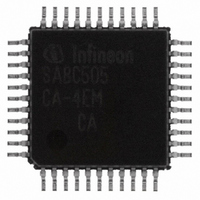
P-MQFP-44-2 (SMD) (Plastic Metric Quad Flat Package) Figure 45 P-MQFP-44 Package Outline Sorts of Packing Package outlines for tubes, trays etc. are contained in our Data Book “Package Information” SMD = Surface Mounted Device Data Sheet C505/C505C/C505A/C505CA 83 Dimensions in ...
Page 88
... Better operating results and business excellence mean less idleness and wastefulness for all of us, more professional success, more accurate information, a better overview and, thereby, less frustration and more satisfaction.” Dr. Ulrich Schumacher Published by Infineon Technologies AG ...