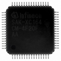
SAK-XC164CM-4F20F AA Infineon Technologies, SAK-XC164CM-4F20F AA Datasheet - Page 58

SAK-XC164CM-4F20F AA
Manufacturer Part Number
SAK-XC164CM-4F20F AA
Description
IC MCU 16BIT 32KB FLSH TQFP-64-8
Manufacturer
Infineon Technologies
Series
XC16xr
Datasheet
1.SAF-XC164CM-4F20F_AA.pdf
(70 pages)
Specifications of SAK-XC164CM-4F20F AA
Core Processor
C166SV2
Core Size
16-Bit
Speed
20MHz
Connectivity
CAN, SPI, UART/USART
Peripherals
PWM, WDT
Number Of I /o
47
Program Memory Size
32KB (32K x 8)
Program Memory Type
FLASH
Ram Size
4K x 8
Voltage - Supply (vcc/vdd)
2.35 V ~ 2.7 V
Data Converters
A/D 14x8/10b
Oscillator Type
Internal
Operating Temperature
-40°C ~ 125°C
Package / Case
64-LFQFP
For Use With
B158-H8961-X-X-7600IN - KIT EASY XC164CMXC164CMUCANIN - KIT U-CAN STARTER XC164CMMCBX167-NET - BOARD EVAL INFINEON CAN/ETHRNTMCBXC167-BASIC - BOARD EVAL BASIC INFINEON XC16X
Lead Free Status / RoHS Status
Lead free / RoHS Compliant
Eeprom Size
-
Other names
KX164CM4F20FAAXT
SAK-XC164CM-4F20F AAINTR
SAK-XC164CM-4F20F AAINTR
SAK-XC164CM-4F20F AATR
SAK-XC164CM-4F20F AATR
SAK-XC164CM-4F20FAA
SAK-XC164CM-4F20FAAINTR
SAK-XC164CM-4F20FAATR
SAKXC164CM4F20FAAXT
SP000084409
SAK-XC164CM-4F20F AAINTR
SAK-XC164CM-4F20F AAINTR
SAK-XC164CM-4F20F AATR
SAK-XC164CM-4F20F AATR
SAK-XC164CM-4F20FAA
SAK-XC164CM-4F20FAAINTR
SAK-XC164CM-4F20FAATR
SAKXC164CM4F20FAAXT
SP000084409
4.3
These parameters describe how the optimum ADC performance can be reached.
Table 14
Parameter
Analog reference supply
Analog reference ground
Analog input voltage range
Basic clock frequency
Conversion time for 10-bit
result
Conversion time for 8-bit
result
Calibration time after reset
Total unadjusted error
Total capacitance
of an analog input
Switched capacitance
of an analog input
Resistance of
the analog input path
Total capacitance
of the reference input
Switched capacitance
of the reference input
Resistance of
the reference input path
1) TUE is tested at
Data Sheet
defined voltage range.
If the analog reference supply voltage drops below 4.5 V (i.e.
voltage by up to 0.2 V (i.e.
subject to production test.
The specified TUE is guaranteed only, if the absolute sum of input overload currents on Port 5 pins (see
specification) does not exceed 10 mA, and if
time. During the reset calibration sequence the maximum TUE may be ±4 LSB.
4)
4)
Analog/Digital Converter Parameters
A/D Converter Characteristics (Operating Conditions apply)
V
AREF
=
V
V
DDP
AREF
+ 0.1 V,
Symbol
V
V
V
f
t
t
t
t
t
TUE
C
C
R
C
C
R
=
BC
C10P
C10
C8P
C8
CAL
AREF
AGND
AIN
AIN
AREF
AINT
AINS
AREFT
AREFS
V
DDP
V
+ 0.2 V) the maximum TUE is increased to ±3 LSB. This range is not
AGND
SR 4.5
SR
SR
CC 52 ×
CC 40 ×
CC 44 ×
CC 32 ×
CC 484
CC –
CC –
CC –
CC –
CC –
CC –
CC –
V
= 0 V. It is verified by design for all other voltages within the
AREF
Min.
V
V
0.5
56
SS
AGND
and
- 0.1
Limit Values
t
t
t
t
V
BC
BC
BC
BC
AGND
+
+
+
+
remain stable during the respective period of
t
t
t
t
V
S
S
S
S
Max.
V
+ 0.1
V
V
20
11,696
±2
15
10
2
20
15
1
AREF
+ 6 ×
+ 6 ×
+ 6 ×
+ 6 ×
DDP
SS
AREF
≥ 4.0 V) or exceeds the power supply
+ 0.1
t
t
t
t
SYS
SYS
SYS
SYS
Electrical Parameters
Unit Test
V
V
V
MHz
–
–
–
–
t
LSB
pF
pF
kΩ
pF
pF
kΩ
BC
Condition
1)
–
2)
3)
Post-calibr. on
Post-calibr. off
Post-calibr. on
Post-calibr. off
5)
1)
6)
6)
6)
6)
6)
6)
Derivatives
V1.4, 2007-03
XC164CM
I
OV


