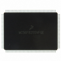
MC56F8355VFGE Freescale Semiconductor, MC56F8355VFGE Datasheet - Page 40

MC56F8355VFGE
Manufacturer Part Number
MC56F8355VFGE
Description
IC DSP 16BIT 60MHZ 128-LQFP
Manufacturer
Freescale Semiconductor
Series
56F8xxxr
Datasheet
1.MC56F8355VFGE.pdf
(172 pages)
Specifications of MC56F8355VFGE
Core Processor
56800
Core Size
16-Bit
Speed
60MHz
Connectivity
CAN, EBI/EMI, SCI, SPI
Peripherals
POR, PWM, Temp Sensor, WDT
Number Of I /o
49
Program Memory Size
264KB (132K x 16)
Program Memory Type
FLASH
Ram Size
10K x 16
Voltage - Supply (vcc/vdd)
2.25 V ~ 3.6 V
Data Converters
A/D 16x12b
Oscillator Type
External
Operating Temperature
-40°C ~ 105°C
Package / Case
128-LQFP
Data Bus Width
16 bit
Processor Series
MC56F83xx
Core
56800E
Numeric And Arithmetic Format
Fixed-Point
Device Million Instructions Per Second
60 MIPs
Maximum Clock Frequency
60 MHz
Number Of Programmable I/os
49
Data Ram Size
20 KB
Maximum Operating Temperature
+ 105 C
Mounting Style
SMD/SMT
Interface Type
SCI, SPI, CAN
Minimum Operating Temperature
- 40 C
For Use With
MC56F8367EVME - EVAL BOARD FOR MC56F83X
Lead Free Status / RoHS Status
Lead free / RoHS Compliant
Eeprom Size
-
Lead Free Status / Rohs Status
Lead free / RoHS Compliant
Available stocks
Company
Part Number
Manufacturer
Quantity
Price
Company:
Part Number:
MC56F8355VFGE
Manufacturer:
Freescale
Quantity:
562
Company:
Part Number:
MC56F8355VFGE
Manufacturer:
Freescale Semiconductor
Quantity:
10 000
Part Number:
MC56F8355VFGE
Manufacturer:
FREESCALE
Quantity:
20 000
5. Not accessible in reset configuration, since the address is above P:$00 FFFF. The higher bit address/GPIO (and/or chip selects)
6. Not accessible in this part, since the EMI is not fully pinned out in this package; information in shaded areas not applicable
7. Two independent program flash blocks allow one to be programmed/erased while executing from another. Each block must have
4.3 Interrupt Vector Table
Table 4-5
organized with higher-priority vectors at the top and lower-priority interrupts lower in the table. The
priority of an interrupt can be assigned to different levels, as indicated, allowing some control over
interrupt priorities. All level 3 interrupts will be serviced before level 2, and so on. For a selected priority
level, the lowest vector number has the highest priority.
The location of the vector table is determined by the Vector Base Address (VBA) register. Please see
5.6.11
In some configurations, the reset address and COP reset address will correspond to vector 0 and 1 of the
interrupt vector table. In these instances, the first two locations in the vector table must contain branch or
JMP instructions. All other entries must contain JSR instructions.
Note: PWMA, FlexCAN, Quadrature Decoder1, and Quad Timers B and D are NOT available on the
56F8155 device.
40
pins must be reconfigured before this external memory is accessible.
to 56F8355/56F8155.
its own mass erase.
core
core
core
core
core
core
core
Peripheral
for the reset value of the VBA.
provides the reset and interrupt priority structure, including on-chip peripherals. The table is
Number
Vector
2
3
4
5
6
7
9
Priority
Table 4-5 Interrupt Vector Table Contents
Level
1-3
1-3
1-3
3
3
3
3
Vector Base
Address +
56F8355 Technical Data, Rev. 17
P:$0A
P:$0C
P:$0E
P:$04
P:$06
P:$08
P:$12
Reserved for Reset Overlay
Reserved for COP Reset Overlay
Illegal Instruction
SW Interrupt 3
HW Stack Overflow
Misaligned Long Word Access
OnCE Step Counter
OnCE Breakpoint Unit 0
Reserved
OnCE Trace Buffer
Interrupt Function
2
1
2
Freescale Semiconductor
Preliminary
Part


