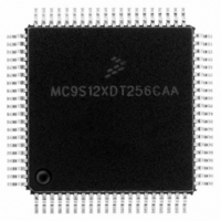
MC9S12XDT256CAA Freescale Semiconductor, MC9S12XDT256CAA Datasheet - Page 636

MC9S12XDT256CAA
Manufacturer Part Number
MC9S12XDT256CAA
Description
IC MCU 256K FLASH 80-QFP
Manufacturer
Freescale Semiconductor
Series
HCS12r
Datasheet
1.MC9S12XD64CAA.pdf
(1348 pages)
Specifications of MC9S12XDT256CAA
Core Processor
HCS12X
Core Size
16-Bit
Speed
80MHz
Connectivity
CAN, EBI/EMI, I²C, IrDA, LIN, SCI, SPI
Peripherals
LVD, POR, PWM, WDT
Number Of I /o
59
Program Memory Size
256KB (256K x 8)
Program Memory Type
FLASH
Eeprom Size
4K x 8
Ram Size
16K x 8
Voltage - Supply (vcc/vdd)
2.35 V ~ 5.5 V
Data Converters
A/D 8x10b
Oscillator Type
External
Operating Temperature
-40°C ~ 85°C
Package / Case
80-QFP
Processor Series
S12XD
Core
HCS12
Data Bus Width
16 bit
Data Ram Size
16 KB
Interface Type
CAN/I2C/SCI/SPI
Maximum Clock Frequency
40 MHz
Number Of Programmable I/os
59
Number Of Timers
12
Maximum Operating Temperature
+ 85 C
Mounting Style
SMD/SMT
3rd Party Development Tools
EWHCS12
Development Tools By Supplier
EVB9S12XDP512E
Minimum Operating Temperature
- 40 C
On-chip Adc
8-ch x 10-bit
Lead Free Status / RoHS Status
Lead free / RoHS Compliant
Available stocks
Company
Part Number
Manufacturer
Quantity
Price
Company:
Part Number:
MC9S12XDT256CAA
Manufacturer:
Freescale Semiconductor
Quantity:
10 000
Company:
Part Number:
MC9S12XDT256CAAR
Manufacturer:
Freescale Semiconductor
Quantity:
10 000
- Current page: 636 of 1348
- Download datasheet (8Mb)
Chapter 17 Memory Mapping Control (S12XMMCV2)
When the device is operating in expanded modes except emulation single-chip mode, accesses to the
global addresses which are not occupied by the on-chip resources (unimplemented areas or external space)
result in accesses to the external bus (see
In emulation single-chip mode, accesses to the global addresses which are not occupied by the on-chip
resources (unimplemented areas) result in accesses to the external bus. CPU accesses to the global
addresses which are occupied by the external space result in an illegal access reset (system reset). The
BDM accesses to the external space are performed but the data is undefined.
In single-chip modes an access to any of the unimplemented areas (see
firmware commands) results in an illegal access reset (system reset). The BDM accesses to the
unimplemented areas are performed but the data is undefined.
Misaligned word accesses to the last location (Top address) of any of the on-chip resource blocks (except
RAM) by the CPU is performed in expanded modes. In single-chip modes these accesses (except Flash)
result in an illegal access reset (except firmware commands).
Misaligned word accesses to the last location (top address) of the on-chip RAM by the CPU is ignored in
expanded modes (read of undefined data). In single-chip modes these accesses result in an illegal access
reset (except firmware commands).
No misaligned word access from the BDM module will occur. These accesses are blocked in the BDM
(Refer to BDM Block Guide).
Misaligned word accesses to the last location of any global page (64 Kbyte) by using global instructions,
is performed by accessing the last byte of the page and the first byte of the same page, considering the
above mentioned misaligned access cases.
The non internal resources (unimplemented areas or external space) are used to generate the chip selects
(CS0,CS1,CS2 and CS3) (see
expanded mode, and special test mode (see
Table 1-21
resources (internal) parameters.
636
1
2
3
4
5
External RPAGE accesses in (NX, EX and ST)
External EPAGE accesses in (NX, EX and ST)
When ROMHM is set (see ROMHM in
memory block.
When the internal NVM is enabled (see ROMON in
the CS0 is not asserted in the space occupied by this on-chip memory block.
External PPAGE accesses in (NX, EX and ST)
shows the address boundaries of each chip select and the relationship with the implemented
Chip Selects
CS2
CS0
CS3
CS2
CS1
3
4
Table 17-20. Global Chip Selects Memory Space
Figure
MC9S12XDP512 Data Sheet, Rev. 2.21
17-23), which are only active in normal expanded mode, emulation
Bottom Address
Table
Figure
$00_0800
$10_0000
$14_0000
$20_0000
$40_0000
Section 1.3.2.1, “MMC Control Register
1-19) the CS2 is asserted in the space occupied by this on-chip
17-23).
Section 1.3.2.5, “MMC Control Register
$13_FFFF minus EEPROMSIZE
$7F_FFFF minus FLASHSIZE
$0F_FFFF minus RAMSIZE
Figure
Top Address
$1F_FFFF
$3F_FFFF
17-23) by the CPU (except
Freescale Semiconductor
(MMCCTL0)”).
(MMCCTL1)”)
1
5
2
Related parts for MC9S12XDT256CAA
Image
Part Number
Description
Manufacturer
Datasheet
Request
R

Part Number:
Description:
16-BIT MICROPROCESSOR FAMILY
Manufacturer:
FREESCALE [Freescale Semiconductor, Inc]
Datasheet:
Part Number:
Description:
Manufacturer:
Freescale Semiconductor, Inc
Datasheet:
Part Number:
Description:
Manufacturer:
Freescale Semiconductor, Inc
Datasheet:
Part Number:
Description:
Manufacturer:
Freescale Semiconductor, Inc
Datasheet:
Part Number:
Description:
Manufacturer:
Freescale Semiconductor, Inc
Datasheet:
Part Number:
Description:
Manufacturer:
Freescale Semiconductor, Inc
Datasheet:
Part Number:
Description:
Manufacturer:
Freescale Semiconductor, Inc
Datasheet:
Part Number:
Description:
Manufacturer:
Freescale Semiconductor, Inc
Datasheet:
Part Number:
Description:
Manufacturer:
Freescale Semiconductor, Inc
Datasheet:
Part Number:
Description:
Manufacturer:
Freescale Semiconductor, Inc
Datasheet:
Part Number:
Description:
Manufacturer:
Freescale Semiconductor, Inc
Datasheet:
Part Number:
Description:
Manufacturer:
Freescale Semiconductor, Inc
Datasheet:
Part Number:
Description:
Manufacturer:
Freescale Semiconductor, Inc
Datasheet:
Part Number:
Description:
Manufacturer:
Freescale Semiconductor, Inc
Datasheet:
Part Number:
Description:
Manufacturer:
Freescale Semiconductor, Inc
Datasheet:


