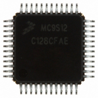
MC9S12C128CFAE Freescale Semiconductor, MC9S12C128CFAE Datasheet - Page 320

MC9S12C128CFAE
Manufacturer Part Number
MC9S12C128CFAE
Description
IC MCU 16BIT 4K FLASH 48-LQFP
Manufacturer
Freescale Semiconductor
Series
HCS12r
Specifications of MC9S12C128CFAE
Core Processor
HCS12
Core Size
16-Bit
Speed
25MHz
Connectivity
CAN, EBI/EMI, SCI, SPI
Peripherals
POR, PWM, WDT
Number Of I /o
31
Program Memory Size
128KB (128K x 8)
Program Memory Type
FLASH
Ram Size
4K x 8
Voltage - Supply (vcc/vdd)
2.35 V ~ 5.5 V
Data Converters
A/D 8x10b
Oscillator Type
Internal
Operating Temperature
-40°C ~ 85°C
Package / Case
48-LQFP
Processor Series
S12C
Core
HCS12
Data Bus Width
16 bit
Data Ram Size
4 KB
Interface Type
CAN/SCI/SPI
Maximum Clock Frequency
25 MHz
Number Of Programmable I/os
31
Number Of Timers
8
Maximum Operating Temperature
+ 85 C
Mounting Style
SMD/SMT
3rd Party Development Tools
EWHCS12
Development Tools By Supplier
M68EVB912C32EE
Minimum Operating Temperature
- 40 C
On-chip Adc
8-ch x 10-bit
Lead Free Status / RoHS Status
Lead free / RoHS Compliant
Eeprom Size
-
Lead Free Status / Rohs Status
Lead free / RoHS Compliant
Available stocks
Company
Part Number
Manufacturer
Quantity
Price
Company:
Part Number:
MC9S12C128CFAE
Manufacturer:
Freescale Semiconductor
Quantity:
10 000
- Current page: 320 of 690
- Download datasheet (4Mb)
Module Base + 0x0004 (DSR0)
Chapter 10 Freescale’s Scalable Controller Area Network (S12MSCANV2)
10.3.3.2
The eight data segment registers, each with bits DB[7:0], contain the data to be transmitted or received.
The number of bytes to be transmitted or received is determined by the data length code in the
corresponding DLR register.
320
Module Base + 0x00X3
DB[7:0]
Field
7:0
Reset:
Reset:
W
W
Figure 10-33. Data Segment Registers (DSR0–DSR7) — Extended Identifier Mapping
R
R
0x0005 (DSR1)
0x0006 (DSR2)
0x0007 (DSR3)
0x0008 (DSR4)
0x0009 (DSR5)
0x000A (DSR6)
0x000B (DSR7)
Data bits 7:0
Data Segment Registers (DSR0-7)
DB7
7
x
7
x
Figure 10-32. Identifier Register 3 — Standard Mapping
= Unused; always read ‘x’
Table 10-30. DSR0–DSR7 Register Field Descriptions
DB6
6
x
6
x
MC9S12C-Family / MC9S12GC-Family
DB5
5
x
5
x
Rev 01.24
DB4
4
x
4
x
Description
DB3
x
x
3
3
DB2
2
x
2
x
Freescale Semiconductor
DB1
x
x
1
1
DB0
0
x
0
x
Related parts for MC9S12C128CFAE
Image
Part Number
Description
Manufacturer
Datasheet
Request
R
Part Number:
Description:
Manufacturer:
Freescale Semiconductor, Inc
Datasheet:
Part Number:
Description:
Manufacturer:
Freescale Semiconductor, Inc
Datasheet:
Part Number:
Description:
Manufacturer:
Freescale Semiconductor, Inc
Datasheet:
Part Number:
Description:
Manufacturer:
Freescale Semiconductor, Inc
Datasheet:
Part Number:
Description:
Manufacturer:
Freescale Semiconductor, Inc
Datasheet:
Part Number:
Description:
Manufacturer:
Freescale Semiconductor, Inc
Datasheet:
Part Number:
Description:
Manufacturer:
Freescale Semiconductor, Inc
Datasheet:
Part Number:
Description:
Manufacturer:
Freescale Semiconductor, Inc
Datasheet:
Part Number:
Description:
Manufacturer:
Freescale Semiconductor, Inc
Datasheet:
Part Number:
Description:
Manufacturer:
Freescale Semiconductor, Inc
Datasheet:
Part Number:
Description:
Manufacturer:
Freescale Semiconductor, Inc
Datasheet:
Part Number:
Description:
Manufacturer:
Freescale Semiconductor, Inc
Datasheet:
Part Number:
Description:
Manufacturer:
Freescale Semiconductor, Inc
Datasheet:
Part Number:
Description:
Manufacturer:
Freescale Semiconductor, Inc
Datasheet:
Part Number:
Description:
Manufacturer:
Freescale Semiconductor, Inc
Datasheet:


