MC9S12C128CFAE Freescale Semiconductor, MC9S12C128CFAE Datasheet - Page 246
MC9S12C128CFAE
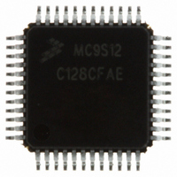
Manufacturer Part Number
MC9S12C128CFAE
Description
IC MCU 16BIT 4K FLASH 48-LQFP
Manufacturer
Freescale Semiconductor
Series
HCS12r
Specifications of MC9S12C128CFAE
Core Processor
HCS12
Core Size
16-Bit
Speed
25MHz
Connectivity
CAN, EBI/EMI, SCI, SPI
Peripherals
POR, PWM, WDT
Number Of I /o
31
Program Memory Size
128KB (128K x 8)
Program Memory Type
FLASH
Ram Size
4K x 8
Voltage - Supply (vcc/vdd)
2.35 V ~ 5.5 V
Data Converters
A/D 8x10b
Oscillator Type
Internal
Operating Temperature
-40°C ~ 85°C
Package / Case
48-LQFP
Processor Series
S12C
Core
HCS12
Data Bus Width
16 bit
Data Ram Size
4 KB
Interface Type
CAN/SCI/SPI
Maximum Clock Frequency
25 MHz
Number Of Programmable I/os
31
Number Of Timers
8
Maximum Operating Temperature
+ 85 C
Mounting Style
SMD/SMT
3rd Party Development Tools
EWHCS12
Development Tools By Supplier
M68EVB912C32EE
Minimum Operating Temperature
- 40 C
On-chip Adc
8-ch x 10-bit
Lead Free Status / RoHS Status
Lead free / RoHS Compliant
Eeprom Size
-
Lead Free Status / Rohs Status
Lead free / RoHS Compliant
Available stocks
Company
Part Number
Manufacturer
Quantity
Price

Company:
Part Number:
MC9S12C128CFAE
Manufacturer:
Freescale Semiconductor
Quantity:
10 000


Chapter 8 Analog-to-Digital Converter (ATD10B8C) Block Description
8.4.2
This subsection explains some of the digital features in more detail. See 7 for all details.
8.4.2.1
The external trigger feature allows the user to synchronize ATD conversions to the external environment
events rather than relying on software to signal the ATD module when ATD conversions are to take place.
The input signal (ATD channel 7) is programmable to be edge or level sensitive with polarity control.
Table 8-19
external trigger function
During a conversion, if additional active edges are detected the overrun error flag ETORF is set.
In either level or edge triggered modes, the first conversion begins when the trigger is received. In both
cases, the maximum latency time is one Bus Clock cycle plus any skew or delay introduced by the trigger
circuitry.
Once ETRIGE is enabled, conversions cannot be started by a write to ATDCTL5, but rather must be
triggered externally.
If the level mode is active and the external trigger both de-asserts and re-asserts itself during a conversion
sequence, this does not constitute an overrun; therefore, the flag is not set. If the trigger is left asserted in
level mode while a sequence is completing, another sequence will be triggered immediately.
246
.
ETRIGLE
X
X
0
0
1
1
gives a brief description of the different combinations of control bits and their affect on the
Digital Sub-block
External Trigger Input (ETRIG)
The conversion results for the external trigger ATD channel 7 have no
meaning while external trigger mode is enabled.
ETRIGP
X
X
0
1
0
1
ETRIGE
Table 8-19. External Trigger Control Bits
0
0
1
1
1
1
MC9S12C-Family / MC9S12GC-Family
SCAN
X
X
X
X
0
1
Rev 01.24
NOTE
Ignores external trigger. Performs one conversion sequence
and stops.
Ignores external trigger. Performs continuous conversion
sequences.
Falling edge triggered. Performs one conversion sequence
per trigger.
Rising edge triggered. Performs one conversion sequence
per trigger.
Trigger active low. Performs continuous conversions while
trigger is active.
Trigger active high. Performs continuous conversions while
trigger is active.
Description
Freescale Semiconductor
Related parts for MC9S12C128CFAE
Image
Part Number
Description
Manufacturer
Datasheet
Request
R

Part Number:
Description:
Manufacturer:
Freescale Semiconductor, Inc
Datasheet:
Part Number:
Description:
Manufacturer:
Freescale Semiconductor, Inc
Datasheet:
Part Number:
Description:
Manufacturer:
Freescale Semiconductor, Inc
Datasheet:
Part Number:
Description:
Manufacturer:
Freescale Semiconductor, Inc
Datasheet:
Part Number:
Description:
Manufacturer:
Freescale Semiconductor, Inc
Datasheet:
Part Number:
Description:
Manufacturer:
Freescale Semiconductor, Inc
Datasheet:
Part Number:
Description:
Manufacturer:
Freescale Semiconductor, Inc
Datasheet:
Part Number:
Description:
Manufacturer:
Freescale Semiconductor, Inc
Datasheet:
Part Number:
Description:
Manufacturer:
Freescale Semiconductor, Inc
Datasheet:
Part Number:
Description:
Manufacturer:
Freescale Semiconductor, Inc
Datasheet:
Part Number:
Description:
Manufacturer:
Freescale Semiconductor, Inc
Datasheet:
Part Number:
Description:
Manufacturer:
Freescale Semiconductor, Inc
Datasheet:
Part Number:
Description:
Manufacturer:
Freescale Semiconductor, Inc
Datasheet:
Part Number:
Description:
Manufacturer:
Freescale Semiconductor, Inc
Datasheet:
Part Number:
Description:
Manufacturer:
Freescale Semiconductor, Inc
Datasheet: