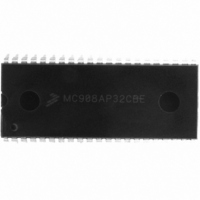
MC908AP32CBE Freescale Semiconductor, MC908AP32CBE Datasheet - Page 86

MC908AP32CBE
Manufacturer Part Number
MC908AP32CBE
Description
IC MCU 32K FLASH 8MHZ 42DIP
Manufacturer
Freescale Semiconductor
Series
HC08r
Specifications of MC908AP32CBE
Core Processor
HC08
Core Size
8-Bit
Speed
8MHz
Connectivity
I²C, IRSCI, SCI, SPI
Peripherals
LED, LVD, POR, PWM
Number Of I /o
30
Program Memory Size
32KB (32K x 8)
Program Memory Type
FLASH
Ram Size
2K x 8
Voltage - Supply (vcc/vdd)
2.7 V ~ 5.5 V
Data Converters
A/D 8x10b
Oscillator Type
Internal
Operating Temperature
-40°C ~ 85°C
Package / Case
42-DIP (0.600", 15.24mm)
Controller Family/series
HC08
No. Of I/o's
30
Ram Memory Size
2KB
Cpu Speed
8MHz
No. Of Timers
2
Embedded Interface Type
I2C, SCI, SPI
Rohs Compliant
Yes
Processor Series
HC08AP
Core
HC08
Data Bus Width
8 bit
Data Ram Size
2 KB
Interface Type
SCI, SPI
Maximum Clock Frequency
8 MHz
Number Of Programmable I/os
32
Number Of Timers
4
Maximum Operating Temperature
+ 85 C
Mounting Style
Through Hole
Development Tools By Supplier
FSICEBASE, DEMO908AP64E, M68CBL05CE
Minimum Operating Temperature
- 40 C
On-chip Adc
10 bit, 8 Channel
Lead Free Status / RoHS Status
Lead free / RoHS Compliant
Eeprom Size
-
Lead Free Status / Rohs Status
Details
- Current page: 86 of 324
- Download datasheet (4Mb)
Clock Generator Module (CGM)
6.3.7 Special Programming Exceptions
The programming method described in
exceptions. A value of 0 for R, N, or L is meaningless when used in the equations given. To account for
these exceptions:
(See
6.3.8 Base Clock Selector Circuit
This circuit is used to select either the oscillator clock, CGMXCLK, or the divided VCO clock, CGMPCLK,
as the source of the base clock, CGMOUT. The two input clocks go through a transition control circuit that
waits up to three CGMXCLK cycles and three CGMPCLK cycles to change from one clock source to the
other. During this time, CGMOUT is held in stasis. The output of the transition control circuit is then
divided by two to correct the duty cycle. Therefore, the bus clock frequency, which is one-half of the base
clock frequency, is one-fourth the frequency of the selected clock (CGMXCLK or CGMPCLK).
The BCS bit in the PLL control register (PCTL) selects which clock drives CGMOUT. The divided VCO
clock cannot be selected as the base clock source if the PLL is not turned on. The PLL cannot be turned
off if the divided VCO clock is selected. The PLL cannot be turned on or off simultaneously with the
selection or deselection of the divided VCO clock. The divided VCO clock also cannot be selected as the
base clock source if the factor L is programmed to a 0. This value would set up a condition inconsistent
with the operation of the PLL, so that the PLL would be disabled and the oscillator clock would be forced
as the source of the base clock.
86
•
•
6.3.8 Base Clock Selector
A 0 value for R or N is interpreted exactly the same as a value of 1.
A 0 value for L disables the PLL and prevents its selection as the source for the base clock.
19.6608 MHz
29.4912 MHz
9.8304 MHz
CGMVCLK
10.0 MHz
8.0 MHz
16 MHz
20 MHz
32 MHz
32 MHz
32 MHz
32 MHz
19.6608 MHz
29.4912 MHz
9.8304 MHz
CGMPCLK
10.0 MHz
8.0 MHz
16 MHz
20 MHz
32 MHz
16 MHz
8 MHz
4 MHz
Circuit.)
MC68HC908AP Family Data Sheet, Rev. 4
Table 6-1. Numeric Examples
6.3.6 Programming the PLL
2.4576 MHz
4.9152 MHz
7.3728 MHz
2.0 MHz
2.5 MHz
4.0 MHz
5.0 MHz
8.0 MHz
4.0 MHz
2.0 MHz
1.0 MHz
f
BUS
32.768 kHz
32.768 kHz
32.768 kHz
32.768 kHz
32.768 kHz
32.768 kHz
32.768 kHz
32.768 kHz
32.768 kHz
32.768 kHz
32.768 kHz
f
RCLK
does not account for three possible
R
1
1
1
1
1
1
1
1
1
1
1
12C
1E9
3D1
1E9
132
258
263
384
F5
F5
7B
N
P
0
0
0
0
0
0
0
0
1
2
3
Freescale Semiconductor
E
0
1
1
1
2
2
2
2
2
2
2
3B
40
27
28
40
27
28
40
40
40
40
L
Related parts for MC908AP32CBE
Image
Part Number
Description
Manufacturer
Datasheet
Request
R
Part Number:
Description:
Manufacturer:
Freescale Semiconductor, Inc
Datasheet:
Part Number:
Description:
Manufacturer:
Freescale Semiconductor, Inc
Datasheet:
Part Number:
Description:
Manufacturer:
Freescale Semiconductor, Inc
Datasheet:
Part Number:
Description:
Manufacturer:
Freescale Semiconductor, Inc
Datasheet:
Part Number:
Description:
Manufacturer:
Freescale Semiconductor, Inc
Datasheet:
Part Number:
Description:
Manufacturer:
Freescale Semiconductor, Inc
Datasheet:
Part Number:
Description:
Manufacturer:
Freescale Semiconductor, Inc
Datasheet:
Part Number:
Description:
Manufacturer:
Freescale Semiconductor, Inc
Datasheet:
Part Number:
Description:
Manufacturer:
Freescale Semiconductor, Inc
Datasheet:
Part Number:
Description:
Manufacturer:
Freescale Semiconductor, Inc
Datasheet:
Part Number:
Description:
Manufacturer:
Freescale Semiconductor, Inc
Datasheet:
Part Number:
Description:
Manufacturer:
Freescale Semiconductor, Inc
Datasheet:
Part Number:
Description:
Manufacturer:
Freescale Semiconductor, Inc
Datasheet:
Part Number:
Description:
Manufacturer:
Freescale Semiconductor, Inc
Datasheet:
Part Number:
Description:
Manufacturer:
Freescale Semiconductor, Inc
Datasheet:


