MCF52213CAE50 Freescale Semiconductor, MCF52213CAE50 Datasheet - Page 25
MCF52213CAE50
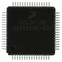
Manufacturer Part Number
MCF52213CAE50
Description
IC MCU 32BIT 128K FLASH 64-LQFP
Manufacturer
Freescale Semiconductor
Series
MCF5221xr
Datasheet
1.MCF52213CAE50.pdf
(56 pages)
Specifications of MCF52213CAE50
Core Processor
Coldfire V2
Core Size
32-Bit
Speed
50MHz
Connectivity
I²C, SPI, UART/USART, USB OTG
Peripherals
DMA, LVD, POR, PWM, WDT
Number Of I /o
56
Program Memory Size
128KB (128K x 8)
Program Memory Type
FLASH
Ram Size
8K x 8
Voltage - Supply (vcc/vdd)
3 V ~ 3.6 V
Data Converters
A/D 8x12b
Oscillator Type
Internal
Operating Temperature
-40°C ~ 85°C
Package / Case
64-LQFP
Processor Series
MCF522x
Core
ColdFire V2
Data Bus Width
32 bit
Data Ram Size
8 KB
Interface Type
I2C, QSPI, UART
Maximum Clock Frequency
50 MHz
Number Of Programmable I/os
43
Number Of Timers
18
Maximum Operating Temperature
+ 85 C
Mounting Style
SMD/SMT
3rd Party Development Tools
JLINK-CF-BDM26, EWCF
Development Tools By Supplier
M52210DEMO, M52211EVB
Minimum Operating Temperature
- 40 C
On-chip Adc
12 bit, 8 Channel
A/d Bit Size
12 bit
A/d Channels Available
8
Height
1.4 mm
Length
10 mm
Supply Voltage (max)
3.6 V
Supply Voltage (min)
3 V
Width
10 mm
For Use With
M52210DEMO - BOARD DEV MCF5221X LOW COST
Lead Free Status / RoHS Status
Lead free / RoHS Compliant
Eeprom Size
-
Lead Free Status / Rohs Status
Details
Available stocks
Company
Part Number
Manufacturer
Quantity
Price
Company:

Part Number:
MCF52213CAE50
Manufacturer:
Freescale Semiconductor
Quantity:
10 000


Family Configurations
1.16
Table 17
25
Processor Status Clock
All Processor Status
Development Serial
Development Serial
Development Serial
Test Data Output
Processor Status
contains a list of EzPort external signals.
Signal Name
Debug Data
Breakpoint
EzPort Signal Descriptions
Outputs
Outputs
Output
Clock
Input
Abbreviation
DDATA[3:0]
PSTCLK
PST[3:0]
ALLPST
DSCLK
BKPT
TDO
DSO
DSI
Table 16. Debug Support Signals (continued)
MCF52211 ColdFire Microcontroller, Rev. 2
Serial output for test instructions and data. TDO is tri-stateable and is
actively driven in the shift-IR and shift-DR controller states. TDO
changes on the falling edge of TCLK.
Development Serial Clock - Internally synchronized input. (The logic
level on DSCLK is validated if it has the same value on two
consecutive rising bus clock edges.) Clocks the serial communication
port to the debug module during packet transfers. Maximum frequency
is PSTCLK/5. At the synchronized rising edge of DSCLK, the data
input on DSI is sampled and DSO changes state.
Breakpoint - Input used to request a manual breakpoint. Assertion of
BKPT puts the processor into a halted state after the current
instruction completes. Halt status is reflected on processor
status/debug data signals (PST[3:0] and PSTDDATA[7:0]) as the
value 0xF. If CSR[BKD] is set (disabling normal BKPT functionality),
asserting BKPT generates a debug interrupt exception in the
processor.
Development Serial Input - Internally synchronized input that provides
data input for the serial communication port to the debug module, after
the DSCLK has been seen as high (logic 1).
Development Serial Output - Provides serial output communication for
debug module responses. DSO is registered internally. The output is
delayed from the validation of DSCLK high.
Display captured processor data and breakpoint status. The CLKOUT
signal can be used by the development system to know when to
sample DDATA[3:0].
Processor Status Clock - Delayed version of the processor clock. Its
rising edge appears in the center of valid PST and DDATA output.
PSTCLK indicates when the development system should sample PST
and DDATA values.
If real-time trace is not used, setting CSR[PCD] keeps PSTCLK, and
PST and DDATA outputs from toggling without disabling triggers.
Non-quiescent operation can be reenabled by clearing CSR[PCD],
although the external development systems must resynchronize with
the PST and DDATA outputs.
PSTCLK starts clocking only when the first non-zero PST value (0xC,
0xD, or 0xF) occurs during system reset exception processing.
Indicate core status. Debug mode timing is synchronous with the
processor clock; status is unrelated to the current bus transfer. The
CLKOUT signal can be used by the development system to know
when to sample PST[3:0].
Logical AND of PST[3:0]. The CLKOUT signal can be used by the
development system to know when to sample ALLPST.
Function
Freescale Semiconductor
I/O
O
O
O
O
O
O
I
I
I
Related parts for MCF52213CAE50
Image
Part Number
Description
Manufacturer
Datasheet
Request
R

Part Number:
Description:
Manufacturer:
Freescale Semiconductor, Inc
Datasheet:
Part Number:
Description:
Manufacturer:
Freescale Semiconductor, Inc
Datasheet:
Part Number:
Description:
Manufacturer:
Freescale Semiconductor, Inc
Datasheet:
Part Number:
Description:
Manufacturer:
Freescale Semiconductor, Inc
Datasheet:
Part Number:
Description:
Manufacturer:
Freescale Semiconductor, Inc
Datasheet:
Part Number:
Description:
Manufacturer:
Freescale Semiconductor, Inc
Datasheet:
Part Number:
Description:
Manufacturer:
Freescale Semiconductor, Inc
Datasheet:
Part Number:
Description:
Manufacturer:
Freescale Semiconductor, Inc
Datasheet:
Part Number:
Description:
Manufacturer:
Freescale Semiconductor, Inc
Datasheet:
Part Number:
Description:
Manufacturer:
Freescale Semiconductor, Inc
Datasheet:
Part Number:
Description:
Manufacturer:
Freescale Semiconductor, Inc
Datasheet:
Part Number:
Description:
Manufacturer:
Freescale Semiconductor, Inc
Datasheet:
Part Number:
Description:
Manufacturer:
Freescale Semiconductor, Inc
Datasheet:
Part Number:
Description:
Manufacturer:
Freescale Semiconductor, Inc
Datasheet:
Part Number:
Description:
Manufacturer:
Freescale Semiconductor, Inc
Datasheet: