R5F21134DFP#U0 Renesas Electronics America, R5F21134DFP#U0 Datasheet - Page 8
R5F21134DFP#U0
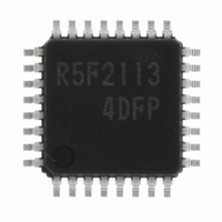
Manufacturer Part Number
R5F21134DFP#U0
Description
IC R8C MCU FLASH 32LQFP
Manufacturer
Renesas Electronics America
Series
M16C™ M16C/R8C/Tiny/13r
Datasheets
1.R5F211A2SPU0.pdf
(300 pages)
2.R5F21132FPU0.pdf
(33 pages)
3.R5F21132FPU0.pdf
(226 pages)
4.R5F21134DFPU0.pdf
(224 pages)
Specifications of R5F21134DFP#U0
Core Size
16-Bit
Program Memory Size
16KB (16K x 8)
Oscillator Type
Internal
Core Processor
R8C
Speed
20MHz
Connectivity
SIO, UART/USART
Peripherals
LED, POR, Voltage Detect, WDT
Number Of I /o
22
Program Memory Type
FLASH
Ram Size
1K x 8
Voltage - Supply (vcc/vdd)
2.7 V ~ 5.5 V
Data Converters
A/D 12x10b
Operating Temperature
-40°C ~ 85°C
Package / Case
32-LQFP
No. Of I/o's
22
Eeprom Memory Size
4KB
Ram Memory Size
1024Byte
Cpu Speed
20MHz
No. Of Timers
16
Digital Ic Case
RoHS Compliant
Controller Family/series
R8C/13
Rohs Compliant
Yes
Lead Free Status / RoHS Status
Lead free / RoHS Compliant
For Use With
R0K521134S000BE - KIT EVAL STARTER FOR R8C/13R0E521134EPB00 - KIT EMULATOR PROBE FOR PC7501R0E521134CPE00 - EMULATOR COMPACT R8C/13
Eeprom Size
-
Lead Free Status / RoHS Status
Lead free / RoHS Compliant
Available stocks
Company
Part Number
Manufacturer
Quantity
Price

Part Number:
R5F21134DFP#U0R5F21134DFP
Manufacturer:
Renesas Electronics America
Quantity:
10 000


R8C/13 Group
Rev.1.20
REJ03B0069-0120
Table 1.3 Pin description
Input port
Power supply
input
IVcc
Analog power
supply input
Reset input
CNVss
MODE
Main clock input
Main clock output X
INT interrupt input
Key input interrupt
input
Timer X
Timer Y
Timer Z
Timer C
Serial interface
Reference voltage V
input
A/D converter
I/O port
_____
1.6 Pin Description
Signal name
Table 1.3 shows the pin description
Jan 27, 2006
Vcc,
Vss
IVcc
AVcc, AVss
RESET
CNVss
MODE
X
INT
_____
KI
CNTR
CNTR
CNTR
TZ
TC
CMP0
CMP1
CLK
RxD
TxD
TxD
AN
P0
P1
P3
P4
P4
_______
___________
__________
IN
OUT
REF
0
page 6 of 27
OUT
0
0
0
5
6
IN
0
Pin name
0
to KI
, P4
0
11
0
0
to P0
to P1
to P3
to AN
, TxD
to INT
, RxD
0
0
_____
0
0
1
to CMP0
to CMP1
7
_______
3
7
7
3
10
11
,
,
, P3
1
3
,
7
2
2
,
, O
I
O
I
I
I
I
I
O
I
I
I/O
O
I/O
O
I
I/O
I
O
I
I
I/O
I
I/O type
Apply 2.7 V to 5.5 V to the Vcc pin. Apply 0 V to the
Vss pin.
This pin is to stabilize internal power supply.
Connect this pin to Vss via a capacitor (0.1 F).
Do not connect to Vcc.
Power supply input pins for A/D converter. Connect the
AVcc pin to Vcc. Connect the AVss pin to Vss. Connect a
capacitor between pins AVcc and AVss.
Input “L” on this pin resets the MCU.
Connect this pin to Vss via a resistor.
Connect this pin to Vcc via a resistor.
These pins are provided for the main clock generat-
ing circuit I/O. Connect a ceramic resonator or a crys-
tal oscillator between the X
an externally derived clock, input it to the X
leave the X
______
INT interrupt input pins.
Key input interrupt pins.
Timer X I/O pin
Timer X output pin
Timer Y I/O pin
Timer Z output pin
Timer C input pin
The timer C output pins
Transfer clock I/O pin.
Serial data input pins.
Serial data output pins.
Reference voltage input pin for A/D converter. Con-
nect the V
Analog input pins for A/D converter
These are 8-bit CMOS I/O ports. Each port has an I/O
select direction register, allowing each pin in that port
to be directed for input or output individually.
Any port set to input can select whether to use a pull-
up resistor or not by program.
P1
Port for input-only
0
to P1
7
REF
OUT
also function as LED drive ports.
pin to Vcc.
pin open.
Function
IN
and X
OUT
pins. To use
IN
1. Overview
pin and
Related parts for R5F21134DFP#U0
Image
Part Number
Description
Manufacturer
Datasheet
Request
R

Part Number:
Description:
KIT STARTER FOR M16C/29
Manufacturer:
Renesas Electronics America
Datasheet:

Part Number:
Description:
KIT STARTER FOR R8C/2D
Manufacturer:
Renesas Electronics America
Datasheet:

Part Number:
Description:
R0K33062P STARTER KIT
Manufacturer:
Renesas Electronics America
Datasheet:

Part Number:
Description:
KIT STARTER FOR R8C/23 E8A
Manufacturer:
Renesas Electronics America
Datasheet:

Part Number:
Description:
KIT STARTER FOR R8C/25
Manufacturer:
Renesas Electronics America
Datasheet:

Part Number:
Description:
KIT STARTER H8S2456 SHARPE DSPLY
Manufacturer:
Renesas Electronics America
Datasheet:

Part Number:
Description:
KIT STARTER FOR R8C38C
Manufacturer:
Renesas Electronics America
Datasheet:

Part Number:
Description:
KIT STARTER FOR R8C35C
Manufacturer:
Renesas Electronics America
Datasheet:

Part Number:
Description:
KIT STARTER FOR R8CL3AC+LCD APPS
Manufacturer:
Renesas Electronics America
Datasheet:
Part Number:
Description:
KIT STARTER FOR RX610
Manufacturer:
Renesas Electronics America
Datasheet:

Part Number:
Description:
KIT STARTER FOR R32C/118
Manufacturer:
Renesas Electronics America
Datasheet:

Part Number:
Description:
KIT DEV RSK-R8C/26-29
Manufacturer:
Renesas Electronics America
Datasheet:

Part Number:
Description:
KIT STARTER FOR SH7124
Manufacturer:
Renesas Electronics America
Datasheet:

Part Number:
Description:
KIT STARTER FOR H8SX/1622
Manufacturer:
Renesas Electronics America
Datasheet:

Part Number:
Description:
KIT DEV FOR SH7203
Manufacturer:
Renesas Electronics America
Datasheet: