C8051F364-GQ Silicon Laboratories Inc, C8051F364-GQ Datasheet - Page 47
C8051F364-GQ
Manufacturer Part Number
C8051F364-GQ
Description
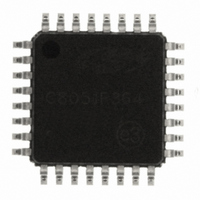
IC 8051 MCU 32K FLASH 32-LQFP
Manufacturer
Silicon Laboratories Inc
Series
C8051F36xr
Specifications of C8051F364-GQ
Program Memory Type
FLASH
Program Memory Size
32KB (32K x 8)
Package / Case
32-LQFP
Core Processor
8051
Core Size
8-Bit
Speed
100MHz
Connectivity
SMBus (2-Wire/I²C), SPI, UART/USART
Peripherals
POR, PWM, Temp Sensor, WDT
Number Of I /o
29
Ram Size
1K x 8
Voltage - Supply (vcc/vdd)
3 V ~ 3.6 V
Oscillator Type
Internal
Operating Temperature
-40°C ~ 85°C
Processor Series
C8051F3x
Core
8051
Data Bus Width
8 bit
Data Ram Size
1 KB
Interface Type
I2C/SMBus/SPI/UART
Maximum Clock Frequency
100 MHz
Number Of Programmable I/os
29
Number Of Timers
4
Maximum Operating Temperature
+ 85 C
Mounting Style
SMD/SMT
3rd Party Development Tools
KSK-SL-TOOLSTICK, PK51, CA51, A51, ULINK2
Development Tools By Supplier
C8051F360DK
Minimum Operating Temperature
- 40 C
Lead Free Status / RoHS Status
Lead free / RoHS Compliant
For Use With
770-1006 - ISP 4PORT FOR SILABS C8051F MCU336-1410 - KIT DEV FOR C8051F360 FAMILY
Eeprom Size
-
Data Converters
-
Lead Free Status / Rohs Status
Lead free / RoHS Compliant
Other names
336-1646
Available stocks
Company
Part Number
Manufacturer
Quantity
Price
Company:

Part Number:
C8051F364-GQ
Manufacturer:
Silicon Labs
Quantity:
135
Company:
Part Number:
C8051F364-GQ
Manufacturer:
SILICON
Quantity:
150
Company:
Part Number:
C8051F364-GQ
Manufacturer:
Silicon Laboratories Inc
Quantity:
10 000
Company:
Part Number:
C8051F364-GQR
Manufacturer:
EVERLIGHT
Quantity:
40 000
Company:
Part Number:
C8051F364-GQR
Manufacturer:
Silicon Laboratories Inc
Quantity:
10 000


5.
The ADC0 subsystem for the C8051F360/1/2/6/7/8/9 consists of two analog multiplexers (referred to col-
lectively as AMUX0) with 23 total input selections, and a 200 ksps, 10-bit successive-approximation-regis-
ter ADC with integrated track-and-hold and programmable window detector. The AMUX0, data conversion
modes, and window detector are all configurable under software control via the Special Function Registers
shown in Figure 5.1. ADC0 operates in both Single-ended and Differential modes, and may be configured
to measure P1.0-P3.4 (where available), the Temperature Sensor output, or V
P3.4, VREF, or GND. The ADC0 subsystem is enabled only when the AD0EN bit in the ADC0 Control reg-
ister (ADC0CN) is set to logic ‘1’. The ADC0 subsystem is in low power shutdown when this bit is logic ‘0’.
P3.1-3.4 available on
P3.1-3.4 available on
P1.0-1.3 available on
C8051F361/2/6/7/8/9
P1.0-1.3 available on
C8051F361/2/6/7/8/9
C8051F360/1/6/8
C8051F360/1/6/8
10-Bit ADC (ADC0, C8051F360/1/2/6/7/8/9)
Sensor
Temp
VREF
GND
VDD
P1.0
P1.7
P2.0
P2.7
P3.0
P3.4
P1.0
P1.7
P2.0
P2.7
P3.0
P3.4
Figure 5.1. ADC0 Functional Block Diagram
23-to-1
23-to-1
AMUX
AMUX
AMX0P
AMX0N
C8051F360/1/2/3/4/5/6/7/8/9
Rev. 1.0
(+)
(-)
ADC0CF
ADC
10-Bit
VDD
SAR
ADC0GTH ADC0GTL
ADC0LTH
ADC0CN
ADC0LTL
DD
Conversion
Start
with respect to P1.0-
000
001
010
011
100
101
32
AD0WINT
Compare
Window
AD0BUSY (W)
Timer 0 Overflow
Timer 2 Overflow
Timer 1 Overflow
CNVSTR Input
Timer 3 Overflow
Logic
47
Related parts for C8051F364-GQ
Image
Part Number
Description
Manufacturer
Datasheet
Request
R

Part Number:
Description:
SMD/C°/SINGLE-ENDED OUTPUT SILICON OSCILLATOR
Manufacturer:
Silicon Laboratories Inc
Part Number:
Description:
Manufacturer:
Silicon Laboratories Inc
Datasheet:
Part Number:
Description:
N/A N/A/SI4010 AES KEYFOB DEMO WITH LCD RX
Manufacturer:
Silicon Laboratories Inc
Datasheet:
Part Number:
Description:
N/A N/A/SI4010 SIMPLIFIED KEY FOB DEMO WITH LED RX
Manufacturer:
Silicon Laboratories Inc
Datasheet:
Part Number:
Description:
N/A/-40 TO 85 OC/EZLINK MODULE; F930/4432 HIGH BAND (REV E/B1)
Manufacturer:
Silicon Laboratories Inc
Part Number:
Description:
EZLink Module; F930/4432 Low Band (rev e/B1)
Manufacturer:
Silicon Laboratories Inc
Part Number:
Description:
I°/4460 10 DBM RADIO TEST CARD 434 MHZ
Manufacturer:
Silicon Laboratories Inc
Part Number:
Description:
I°/4461 14 DBM RADIO TEST CARD 868 MHZ
Manufacturer:
Silicon Laboratories Inc
Part Number:
Description:
I°/4463 20 DBM RFSWITCH RADIO TEST CARD 460 MHZ
Manufacturer:
Silicon Laboratories Inc
Part Number:
Description:
I°/4463 20 DBM RADIO TEST CARD 868 MHZ
Manufacturer:
Silicon Laboratories Inc
Part Number:
Description:
I°/4463 27 DBM RADIO TEST CARD 868 MHZ
Manufacturer:
Silicon Laboratories Inc
Part Number:
Description:
I°/4463 SKYWORKS 30 DBM RADIO TEST CARD 915 MHZ
Manufacturer:
Silicon Laboratories Inc
Part Number:
Description:
N/A N/A/-40 TO 85 OC/4463 RFMD 30 DBM RADIO TEST CARD 915 MHZ
Manufacturer:
Silicon Laboratories Inc
Part Number:
Description:
I°/4463 20 DBM RADIO TEST CARD 169 MHZ
Manufacturer:
Silicon Laboratories Inc