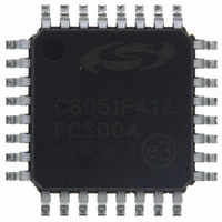
C8051F412-GQ Silicon Laboratories Inc, C8051F412-GQ Datasheet - Page 33

C8051F412-GQ
Manufacturer Part Number
C8051F412-GQ
Description
IC 8051 MCU 16K FLASH 32LQFP
Manufacturer
Silicon Laboratories Inc
Series
C8051F41xr
Specifications of C8051F412-GQ
Program Memory Type
FLASH
Program Memory Size
16KB (16K x 8)
Package / Case
32-LQFP
Core Processor
8051
Core Size
8-Bit
Speed
50MHz
Connectivity
SMBus (2-Wire/I²C), SPI, UART/USART
Peripherals
Brown-out Detect/Reset, POR, PWM, Temp Sensor, WDT
Number Of I /o
24
Ram Size
2.25K x 8
Voltage - Supply (vcc/vdd)
2 V ~ 5.25 V
Data Converters
A/D 20x12b; D/A 2x12b
Oscillator Type
Internal
Operating Temperature
-40°C ~ 85°C
Processor Series
C8051F4x
Core
8051
Data Bus Width
8 bit
Data Ram Size
2.25 KB
Interface Type
I2C/SMBus/SPI/UART
Maximum Clock Frequency
50 MHz
Number Of Programmable I/os
24
Number Of Timers
4
Operating Supply Voltage
2 V to 5.25 V
Maximum Operating Temperature
+ 85 C
Mounting Style
SMD/SMT
3rd Party Development Tools
PK51, CA51, A51, ULINK2
Development Tools By Supplier
C8051F410DK
Minimum Operating Temperature
- 40 C
On-chip Dac
2-ch x 12-bit
No. Of I/o's
24
Ram Memory Size
2368Byte
Cpu Speed
50MHz
No. Of Timers
4
Rohs Compliant
Yes
Package
32LQFP
Device Core
8051
Family Name
C8051F41x
Maximum Speed
50 MHz
Lead Free Status / RoHS Status
Lead free / RoHS Compliant
For Use With
770-1006 - ISP 4PORT FOR SILABS C8051F MCU336-1453 - ADAPTER PROGRAM TOOLSTICK F410336-1317 - KIT EVAL FOR C8051F411336-1314 - KIT DEV FOR C8051F41X
Eeprom Size
-
Lead Free Status / Rohs Status
Lead free / RoHS Compliant
Other names
336-1310
Available stocks
Company
Part Number
Manufacturer
Quantity
Price
Company:
Part Number:
C8051F412-GQ
Manufacturer:
Silicon Laboratories Inc
Quantity:
10 000
Company:
Part Number:
C8051F412-GQR
Manufacturer:
Silicon Laboratories Inc
Quantity:
10 000
- Current page: 33 of 270
- Download datasheet (2Mb)
1.12. Port Input/Output
C8051F41x devices include up to 24 I/O pins. Port pins are organized as three byte-wide ports. The port
pins behave like typical 8051 ports with a few enhancements. Each port pin can be configured as a digital
or analog I/O pin. Pins selected as digital I/O can be configured for push-pull or open-drain operation. The
“weak pullups” that are fixed on typical 8051 devices may be individually or globally disabled to save
power.
The Digital Crossbar allows mapping of internal digital system resources to port I/O pins. On-chip coun-
ter/timers, serial buses, hardware interrupts, and other digital signals can be configured to appear on the
port pins using the Crossbar control registers. This allows the user to select the exact mix of general-pur-
pose port I/O, digital, and analog resources needed for the application.
Highest
Priority
Lowest
Priority
SYSCLK
Outputs
SMBus
T0, T1
UART
P0
P1
P2
PCA
CP0
CP1
SPI
(P0.0-P0.7)
(P1.0-P1.7)
(P2.0-P2.7)
Figure 1.11. Port I/O Functional Block Diagram
2
4
2
4
7
2
8
8
8
Rev. 1.1
PnSKIP Registers
XBR0, XBR1,
Crossbar
Decoder
Priority
Digital
8
8
8
P0MASK, P0MATCH
P1MASK, P1MATCH
C8051F410/1/2/3
Registers
Cells
Cells
Cell
I/O
I/O
I/O
P0
P1
P2
P2.3–2.6 available on
PnMDIN Registers
C8051F410/2
PnMDOUT,
P0.0
P0.7
P1.0
P1.7
P2.0
P2.7
33
Related parts for C8051F412-GQ
Image
Part Number
Description
Manufacturer
Datasheet
Request
R
Part Number:
Description:
SMD/C°/SINGLE-ENDED OUTPUT SILICON OSCILLATOR
Manufacturer:
Silicon Laboratories Inc
Part Number:
Description:
Manufacturer:
Silicon Laboratories Inc
Datasheet:
Part Number:
Description:
N/A N/A/SI4010 AES KEYFOB DEMO WITH LCD RX
Manufacturer:
Silicon Laboratories Inc
Datasheet:
Part Number:
Description:
N/A N/A/SI4010 SIMPLIFIED KEY FOB DEMO WITH LED RX
Manufacturer:
Silicon Laboratories Inc
Datasheet:
Part Number:
Description:
N/A/-40 TO 85 OC/EZLINK MODULE; F930/4432 HIGH BAND (REV E/B1)
Manufacturer:
Silicon Laboratories Inc
Part Number:
Description:
EZLink Module; F930/4432 Low Band (rev e/B1)
Manufacturer:
Silicon Laboratories Inc
Part Number:
Description:
I°/4460 10 DBM RADIO TEST CARD 434 MHZ
Manufacturer:
Silicon Laboratories Inc
Part Number:
Description:
I°/4461 14 DBM RADIO TEST CARD 868 MHZ
Manufacturer:
Silicon Laboratories Inc
Part Number:
Description:
I°/4463 20 DBM RFSWITCH RADIO TEST CARD 460 MHZ
Manufacturer:
Silicon Laboratories Inc
Part Number:
Description:
I°/4463 20 DBM RADIO TEST CARD 868 MHZ
Manufacturer:
Silicon Laboratories Inc
Part Number:
Description:
I°/4463 27 DBM RADIO TEST CARD 868 MHZ
Manufacturer:
Silicon Laboratories Inc
Part Number:
Description:
I°/4463 SKYWORKS 30 DBM RADIO TEST CARD 915 MHZ
Manufacturer:
Silicon Laboratories Inc
Part Number:
Description:
N/A N/A/-40 TO 85 OC/4463 RFMD 30 DBM RADIO TEST CARD 915 MHZ
Manufacturer:
Silicon Laboratories Inc
Part Number:
Description:
I°/4463 20 DBM RADIO TEST CARD 169 MHZ
Manufacturer:
Silicon Laboratories Inc


