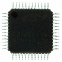
C8051F505-IQ Silicon Laboratories Inc, C8051F505-IQ Datasheet - Page 207

C8051F505-IQ
Manufacturer Part Number
C8051F505-IQ
Description
IC 8051 MCU 32K FLASH 48-QFP
Manufacturer
Silicon Laboratories Inc
Series
C8051F50xr
Specifications of C8051F505-IQ
Program Memory Type
FLASH
Program Memory Size
32KB (32K x 8)
Package / Case
48-QFP
Mfg Application Notes
LIN Bootloader AppNote
Core Processor
8051
Core Size
8-Bit
Speed
50MHz
Connectivity
EBI/EMI, SMBus (2-Wire/I²C), SPI, UART/USART
Peripherals
POR, PWM, Temp Sensor, WDT
Number Of I /o
40
Ram Size
4.25K x 8
Voltage - Supply (vcc/vdd)
1.8 V ~ 5.25 V
Data Converters
A/D 32x12b
Oscillator Type
Internal
Operating Temperature
-40°C ~ 125°C
Processor Series
C8051F5x
Core
8051
Data Bus Width
8 bit
Data Ram Size
4.25 KB
Interface Type
I2C/SPI/UART
Maximum Clock Frequency
50 MHz
Number Of Programmable I/os
40
Number Of Timers
4
Maximum Operating Temperature
+ 125 C
Mounting Style
SMD/SMT
3rd Party Development Tools
PK51, CA51, A51, ULINK2
Development Tools By Supplier
C8051F500DK
Minimum Operating Temperature
- 40 C
On-chip Adc
32-ch x 12-bit
Package
48PQFP
Device Core
8051
Family Name
C8051F50x
Maximum Speed
50 MHz
Operating Supply Voltage
2.5|3.3|5 V
Lead Free Status / RoHS Status
Lead free / RoHS Compliant
For Use With
336-1527 - KIT DEV FOR C8051F50X
Eeprom Size
-
Lead Free Status / Rohs Status
Lead free / RoHS Compliant
Other names
336-1520
Available stocks
Company
Part Number
Manufacturer
Quantity
Price
Company:
Part Number:
C8051F505-IQ
Manufacturer:
SLB
Quantity:
590
Company:
Part Number:
C8051F505-IQ
Manufacturer:
Silicon Laboratories Inc
Quantity:
10 000
Company:
Part Number:
C8051F505-IQR
Manufacturer:
Silicon Laboratories Inc
Quantity:
10 000
- Current page: 207 of 312
- Download datasheet (3Mb)
4. Changing the configuration of the checksum during a transaction will cause the interface to reset and
21.5. Sleep Mode and Wake-Up
To reduce the system’s power consumption, the LIN Protocol Specification defines a Sleep Mode. The
message used to broadcast a Sleep Mode request must be transmitted by the LIN master application in
the same way as a normal transmit message. The LIN slave application must decode the Sleep Mode
Frame from the Identifier and data bytes. After that, it has to put the LIN slave node into the Sleep Mode by
setting the SLEEP bit (LIN0CTRL.6).
If the SLEEP bit (LIN0CTRL.6) of the LIN slave application is not set and there is no bus activity for four
seconds (specified bus idle timeout), the IDLTOUT bit (LIN0ST.6) is set and an interrupt request is gener-
ated. After that the application may assume that the LIN bus is in Sleep Mode and set the SLEEP bit
(LIN0CTRL.6).
Sending a wake-up signal from the master or any slave node terminates the Sleep Mode of the LIN bus. To
send a wake-up signal, the application has to set the WUPREQ bit (LIN0CTRL.1). After successful trans-
mission of the wake-up signal, the DONE bit (LIN0ST.0) of the master node is set and an interrupt request
is generated. The LIN slave does not generate an interrupt request after successful transmission of the
wake-up signal but it generates an interrupt request if the master does not respond to the wake-up signal
within 150 milliseconds. In that case, the ERROR bit (LIN0ST.2) and TOUT bit (LIN0ERR.2) are set. The
application then has to decide whether or not to transmit another wake-up signal.
All LIN nodes that detect a wake-up signal will set the WAKEUP (LIN0ST.1) and DONE bits (LIN0ST.0) and
generate an interrupt request. After that, the application has to clear the SLEEP bit (LIN0CTRL.6) in the
LIN slave.
21.6. Error Detection and Handling
The LIN controller generates an interrupt request and stops the processing of the current frame if it detects
an error. The application has to check the type of error by processing LIN0ERR. After that, it has to reset
the error register and the ERROR bit (LIN0ST.2) by writing a 1 to the RSTERR bit (LIN0CTRL.2). Starting a
new message with the LIN controller selected as master or sending a Wakeup signal with the LIN control-
ler selected as a master or slave is possible only if the ERROR bit (LIN0ST.2) is set to 0.
of setting the DTACK (LIN0CTRL.4) bit. At that time, steps 2 through 5 can then be skipped. In this
situation, the LIN controller stops the processing of LIN communication until the next SYNC BREAK is
received.
the transaction to be lost. To prevent this, the checksum should not be configured while a transaction is
in progress. The same applies to changes in the LIN interface mode from slave mode to master mode
and from master mode to slave mode.
Rev. 1.2
C8051F50x/F51x
207
Related parts for C8051F505-IQ
Image
Part Number
Description
Manufacturer
Datasheet
Request
R
Part Number:
Description:
SMD/C°/SINGLE-ENDED OUTPUT SILICON OSCILLATOR
Manufacturer:
Silicon Laboratories Inc
Part Number:
Description:
Manufacturer:
Silicon Laboratories Inc
Datasheet:
Part Number:
Description:
N/A N/A/SI4010 AES KEYFOB DEMO WITH LCD RX
Manufacturer:
Silicon Laboratories Inc
Datasheet:
Part Number:
Description:
N/A N/A/SI4010 SIMPLIFIED KEY FOB DEMO WITH LED RX
Manufacturer:
Silicon Laboratories Inc
Datasheet:
Part Number:
Description:
N/A/-40 TO 85 OC/EZLINK MODULE; F930/4432 HIGH BAND (REV E/B1)
Manufacturer:
Silicon Laboratories Inc
Part Number:
Description:
EZLink Module; F930/4432 Low Band (rev e/B1)
Manufacturer:
Silicon Laboratories Inc
Part Number:
Description:
I°/4460 10 DBM RADIO TEST CARD 434 MHZ
Manufacturer:
Silicon Laboratories Inc
Part Number:
Description:
I°/4461 14 DBM RADIO TEST CARD 868 MHZ
Manufacturer:
Silicon Laboratories Inc
Part Number:
Description:
I°/4463 20 DBM RFSWITCH RADIO TEST CARD 460 MHZ
Manufacturer:
Silicon Laboratories Inc
Part Number:
Description:
I°/4463 20 DBM RADIO TEST CARD 868 MHZ
Manufacturer:
Silicon Laboratories Inc
Part Number:
Description:
I°/4463 27 DBM RADIO TEST CARD 868 MHZ
Manufacturer:
Silicon Laboratories Inc
Part Number:
Description:
I°/4463 SKYWORKS 30 DBM RADIO TEST CARD 915 MHZ
Manufacturer:
Silicon Laboratories Inc
Part Number:
Description:
N/A N/A/-40 TO 85 OC/4463 RFMD 30 DBM RADIO TEST CARD 915 MHZ
Manufacturer:
Silicon Laboratories Inc
Part Number:
Description:
I°/4463 20 DBM RADIO TEST CARD 169 MHZ
Manufacturer:
Silicon Laboratories Inc


