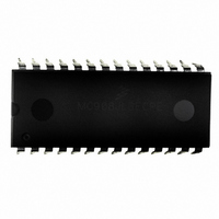
MC908JL3ECPE Freescale Semiconductor, MC908JL3ECPE Datasheet - Page 80

MC908JL3ECPE
Manufacturer Part Number
MC908JL3ECPE
Description
IC MCU 4K FLASH 8MHZ 28-DIP
Manufacturer
Freescale Semiconductor
Series
HC08r
Specifications of MC908JL3ECPE
Core Processor
HC08
Core Size
8-Bit
Speed
8MHz
Peripherals
LED, LVD, POR, PWM
Number Of I /o
23
Program Memory Size
4KB (4K x 8)
Program Memory Type
FLASH
Ram Size
128 x 8
Voltage - Supply (vcc/vdd)
2.7 V ~ 3.3 V
Data Converters
A/D 12x8b
Oscillator Type
External
Operating Temperature
-40°C ~ 85°C
Package / Case
28-DIP (0.600", 15.24mm)
Controller Family/series
HC08
No. Of I/o's
23
Ram Memory Size
128Byte
Cpu Speed
8MHz
No. Of Timers
1
Rohs Compliant
Yes
Processor Series
HC08JL
Core
HC08
Data Bus Width
8 bit
Data Ram Size
128 B
Maximum Clock Frequency
8 MHz
Number Of Programmable I/os
26
Number Of Timers
2
Operating Supply Voltage
3 V to 5 V
Maximum Operating Temperature
+ 85 C
Mounting Style
Through Hole
Development Tools By Supplier
FSICEBASE, DEMO908JL16E, M68CBL05CE
Minimum Operating Temperature
- 40 C
On-chip Adc
8 bit, 12 Channel
Lead Free Status / RoHS Status
Lead free / RoHS Compliant
Eeprom Size
-
Connectivity
-
Lead Free Status / Rohs Status
Details
Available stocks
Company
Part Number
Manufacturer
Quantity
Price
Part Number:
MC908JL3ECPE
Manufacturer:
FREESCALE
Quantity:
20 000
Monitor ROM (MON)
Upon power-on reset, if the received bytes of the security code do not match the data at locations
$FFF6–$FFFD, the host fails to bypass the security feature. The MCU remains in monitor mode, but
reading a Flash location returns an invalid value and trying to execute code from Flash causes an illegal
address reset. After receiving the eight security bytes from the host, the MCU transmits a break character,
signifying that it is ready to receive a command.
To determine whether the security code entered is correct, check to see if bit 6 of RAM address $80 is
set. If it is, then the correct security code has been entered and Flash can be accessed.
If the security sequence fails, the device should be reset by a power-on reset and brought up in monitor
mode to attempt another entry. After failing the security sequence, the Flash module can also be mass
erased by executing an erase routine that was downloaded into internal RAM. The mass erase operation
clears the security code locations so that all eight security bytes become $FF (blank).
80
PTB0
V
RST
NOTES:
The MCU does not transmit a break character until after the host sends the
eight security bytes.
DD
1 = Echo delay, 2 bit times
2 = Data return delay, 2 bit times
4 = Wait 1 bit time before sending next byte.
FROM HOST
FROM MCU
Figure 7-7. Monitor Mode Entry Timing
4096 + 32 OSCXCLK CYCLES
MC68HC908JL3E Family Data Sheet, Rev. 4
24 BUS CYCLES
1
NOTE
4
1
1
2
4
Freescale Semiconductor
1


