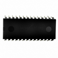
MC908JL3ECPE Freescale Semiconductor, MC908JL3ECPE Datasheet - Page 33

MC908JL3ECPE
Manufacturer Part Number
MC908JL3ECPE
Description
IC MCU 4K FLASH 8MHZ 28-DIP
Manufacturer
Freescale Semiconductor
Series
HC08r
Specifications of MC908JL3ECPE
Core Processor
HC08
Core Size
8-Bit
Speed
8MHz
Peripherals
LED, LVD, POR, PWM
Number Of I /o
23
Program Memory Size
4KB (4K x 8)
Program Memory Type
FLASH
Ram Size
128 x 8
Voltage - Supply (vcc/vdd)
2.7 V ~ 3.3 V
Data Converters
A/D 12x8b
Oscillator Type
External
Operating Temperature
-40°C ~ 85°C
Package / Case
28-DIP (0.600", 15.24mm)
Controller Family/series
HC08
No. Of I/o's
23
Ram Memory Size
128Byte
Cpu Speed
8MHz
No. Of Timers
1
Rohs Compliant
Yes
Processor Series
HC08JL
Core
HC08
Data Bus Width
8 bit
Data Ram Size
128 B
Maximum Clock Frequency
8 MHz
Number Of Programmable I/os
26
Number Of Timers
2
Operating Supply Voltage
3 V to 5 V
Maximum Operating Temperature
+ 85 C
Mounting Style
Through Hole
Development Tools By Supplier
FSICEBASE, DEMO908JL16E, M68CBL05CE
Minimum Operating Temperature
- 40 C
On-chip Adc
8 bit, 12 Channel
Lead Free Status / RoHS Status
Lead free / RoHS Compliant
Eeprom Size
-
Connectivity
-
Lead Free Status / Rohs Status
Details
Available stocks
Company
Part Number
Manufacturer
Quantity
Price
Part Number:
MC908JL3ECPE
Manufacturer:
FREESCALE
Quantity:
20 000
2.12 Flash Block Protect Register
The Flash Block Protect Register is implemented as an 8-bit I/O register. The value in this register
determines the starting address of the protected range within the Flash memory.
BPR[7:0] — Flash Block Protect Register Bit 7 to Bit 0
Freescale Semiconductor
BPR[7:1] represent bits [12:6] of a 16-bit memory address. Bits [15:13] are 1’s and bits [5:0] are 0’s.
BPR0 is used only for BPR[7:0] = $FF, for no block protection.
The resultant 16-bit address is used for specifying the start address of the Flash memory for block
protection. The Flash is protected from this start address to the end of Flash memory, at $FFFF. With
this mechanism, the protect start address can be XX00, XX40, XX80, or XXC0 (at page boundaries —
64 bytes) within the Flash memory.
Examples of protect start address:
Address:
Reset:
Read:
Write:
Start address of Flash block protect
and so on...
Note:
The end address of the protected range is always $FFFF.
$FE09
BPR7
(0110 001x)
(0110 010x)
(0110 100x)
$DE or $DF
(1101 111x)
(1111 1110)
Bit 7
$62 or $63
$64 or $65
$68 or $69
BPR[7:0]
0
$00–$60
Figure 2-6. Flash Block Protect Register (FLBPR)
$FE
$FF
BPR6
MC68HC908JL3E Family Data Sheet, Rev. 4
6
0
BPR5
5
0
The entire Flash memory is not protected.
The entire Flash memory is protected.
Start of Address of Protect Range
BPR4
$FBC0 (1111 1011 1100 0000)
$EC40 (1110 1100 0100 0000)
$EC80 (1110 1100 1000 0000)
$ED00 (1110 1101 0000 0000)
$FFC0 (1111 1111 1100 0000)
1 1 1
4
0
BPR3
3
0
16-bit memory address
BPR[7:1]
BPR2
2
0
BPR1
0 0 0 0 0 0
1
0
Flash Block Protect Register
BPR0
Bit 0
0
33


