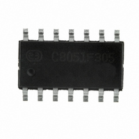
C8051F305-GS Silicon Laboratories Inc, C8051F305-GS Datasheet - Page 65

C8051F305-GS
Manufacturer Part Number
C8051F305-GS
Description
IC 8051 MCU 2K FLASH 14-SOIC
Manufacturer
Silicon Laboratories Inc
Series
C8051F30xr
Specifications of C8051F305-GS
Program Memory Type
FLASH
Program Memory Size
2KB (2K x 8)
Package / Case
14-SOIC (3.9mm Width), 14-SOL
Core Processor
8051
Core Size
8-Bit
Speed
25MHz
Connectivity
SMBus (2-Wire/I²C), UART/USART
Peripherals
POR, PWM, WDT
Number Of I /o
8
Ram Size
256 x 8
Voltage - Supply (vcc/vdd)
2.7 V ~ 3.6 V
Oscillator Type
External
Operating Temperature
-40°C ~ 85°C
Processor Series
C8051F3x
Core
8051
Data Bus Width
8 bit
Data Ram Size
256 B
Interface Type
I2C/SMBus/UART
Maximum Clock Frequency
25 MHz
Number Of Programmable I/os
8
Number Of Timers
3
Maximum Operating Temperature
+ 85 C
Mounting Style
SMD/SMT
3rd Party Development Tools
PK51, CA51, A51, ULINK2
Development Tools By Supplier
C8051F300DK
Minimum Operating Temperature
- 40 C
Lead Free Status / RoHS Status
Lead free / RoHS Compliant
For Use With
770-1006 - ISP 4PORT FOR SILABS C8051F MCU336-1444 - ADAPTER PROGRAM TOOLSTICK F300
Eeprom Size
-
Data Converters
-
Lead Free Status / Rohs Status
Lead free / RoHS Compliant
Other names
336-1540-5
C8051F300/1/2/3/4/5
8.2.4. Bit Addressable Locations
In addition to direct access to data memory organized as bytes, the sixteen data memory locations at 0x20
through 0x2F are also accessible as 128 individually addressable bits. Each bit has a bit address from
0x00 to 0x7F. Bit 0 of the byte at 0x20 has bit address 0x00 while bit 7 of the byte at 0x20 has bit address
0x07. Bit 7 of the byte at 0x2F has bit address 0x7F. A bit access is distinguished from a full byte access by
the type of instruction used (bit source or destination operands as opposed to a byte source or destina-
tion).
The MCS-51™ assembly language allows an alternate notation for bit addressing of the form XX.B where
XX is the byte address and B is the bit position within the byte. For example, the instruction:
MOV
C, 22.3h
moves the Boolean value at 0x13 (bit 3 of the byte at location 0x22) into the Carry flag.
8.2.5. Stack
A programmer's stack can be located anywhere in the 256-byte data memory. The stack area is desig-
nated using the Stack Pointer (SP, 0x81) SFR. The SP will point to the last location used. The next value
pushed on the stack is placed at SP+1 and then SP is incremented. A reset initializes the stack pointer to
location 0x07. Therefore, the first value pushed on the stack is placed at location 0x08, which is also the
first register (R0) of register bank 1. Thus, if more than one register bank is to be used, the SP should be
initialized to a location in the data memory not being used for data storage. The stack depth can extend up
to 256 bytes.
8.2.6. Special Function Registers
The direct-access data memory locations from 0x80 to 0xFF constitute the special function registers
(SFRs). The SFRs provide control and data exchange with the CIP-51's resources and peripherals. The
CIP-51 duplicates the SFRs found in a typical 8051 implementation as well as implementing additional
SFRs used to configure and access the subsystems unique to the MCU. This allows the addition of new
functionality while retaining compatibility with the MCS-51™ instruction set. Table 8.2 lists the SFRs imple-
mented in the CIP-51 System Controller.
The SFR registers are accessed anytime the direct addressing mode is used to access memory locations
from 0x80 to 0xFF. SFRs with addresses ending in 0x0 or 0x8 (e.g. P0, TCON, SCON0, IE, etc.) are bit-
addressable as well as byte-addressable. All other SFRs are byte-addressable only. Unoccupied
addresses in the SFR space are reserved for future use. Accessing these areas will have an indeterminate
effect and should be avoided. Refer to the corresponding pages of the datasheet, as indicated in Table 8.3,
for a detailed description of each register.
Rev. 2.9
65


