STM32F103C4T6A STMicroelectronics, STM32F103C4T6A Datasheet - Page 59
STM32F103C4T6A
Manufacturer Part Number
STM32F103C4T6A
Description
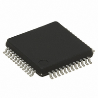
MCU ARM 32BIT 16K FLASH 48-LQFP
Manufacturer
STMicroelectronics
Series
STM32r
Datasheet
1.STM32F103C4T6A.pdf
(87 pages)
Specifications of STM32F103C4T6A
Core Processor
ARM® Cortex-M3™
Core Size
32-Bit
Speed
72MHz
Connectivity
CAN, I²C, IrDA, LIN, SPI, UART/USART, USB
Peripherals
DMA, Motor Control PWM, PDR, POR, PVD, PWM, Temp Sensor, WDT
Number Of I /o
26
Program Memory Size
16KB (16K x 8)
Program Memory Type
FLASH
Ram Size
6K x 8
Voltage - Supply (vcc/vdd)
2 V ~ 3.6 V
Data Converters
A/D 10x12b
Oscillator Type
Internal
Operating Temperature
-40°C ~ 85°C
Package / Case
48-LQFP
For Use With
497-10048 - BOARD EVAL ACCELEROMETER497-10030 - STARTER KIT FOR STM32497-8853 - BOARD DEMO STM32 UNIV USB-UUSCIKSDKSTM32-PL - KIT IAR KICKSTART STM32 CORTEXM3497-8512 - KIT STARTER FOR STM32F10XE MCU497-8511 - KIT STARTER FOR STM32 512K FLASH497-8505 - KIT STARTER FOR STM32F10XE MCU497-8304 - KIT STM32 MOTOR DRIVER BLDC497-6438 - BOARD EVALUTION FOR STM32 512K497-6289 - KIT PERFORMANCE STICK FOR STM32MCBSTM32UME - BOARD EVAL MCBSTM32 + ULINK-MEMCBSTM32U - BOARD EVAL MCBSTM32 + ULINK2MCBSTM32 - BOARD EVAL FOR STM STM32X SER497-6053 - KIT STARTER FOR STM32497-6052 - KIT STARTER FOR STM32497-6050 - KIT STARTER FOR STM32497-6049 - KIT EVALUATION LOW COST STM32497-6048 - BOARD EVALUATION FOR STM32497-6047 - KIT DEVELOPMENT FOR STM32497-5046 - KIT TOOL FOR ST7/UPSD/STR7 MCU
Lead Free Status / RoHS Status
Lead free / RoHS Compliant
Eeprom Size
-
Lead Free Status / Rohs Status
Details
Other names
497-8316
Available stocks
Company
Part Number
Manufacturer
Quantity
Price
Company:

Part Number:
STM32F103C4T6A
Manufacturer:
STMicroelectronics
Quantity:
99
Company:
Part Number:
STM32F103C4T6A
Manufacturer:
STMicroelectronics
Quantity:
10 000


STM32F103x4, STM32F103x6
Output driving current
The GPIOs (general-purpose inputs/outputs) can sink or source up to ±8 mA, and sink or
source up to ±20 mA (with a relaxed V
In the user application, the number of I/O pins which can drive current must be limited to
respect the absolute maximum rating specified in
●
●
Output voltage levels
Unless otherwise specified, the parameters given in
performed under ambient temperature and V
Table
Table 36.
1. The I
2. TTL and CMOS outputs are compatible with JEDEC standards JESD36 and JESD52.
3. The I
4. Based on characterization data, not tested in production.
V
V
Symbol
V
V
V
V
V
V
OH
OH
OL
OL
OH
OL
OH
and the sum of I
Table 7
OL
(1)(4)
(1)(4)
(3)(4)
(3)(4)
The sum of the currents sourced by all the I/Os on V
consumption of the MCU sourced on V
I
The sum of the currents sunk by all the I/Os on V
consumption of the MCU sunk on V
I
VDD
VSS
(1)
(3)
(1)
(3)
9. All I/Os are CMOS and TTL compliant.
IO
IO
current sunk by the device must always respect the absolute maximum rating specified in
current sourced by the device must always respect the absolute maximum rating specified in
(see
and the sum of I
(see
Output low level voltage for an I/O pin
when 8 pins are sunk at same time
Output high level voltage for an I/O pin
when 8 pins are sourced at same time
Output low level voltage for an I/O pin
when 8 pins are sunk at same time
Output high level voltage for an I/O pin
when 8 pins are sourced at same time
Output low level voltage for an I/O pin
when 8 pins are sunk at same time
Output high level voltage for an I/O pin
when 8 pins are sourced at same time
Output low level voltage for an I/O pin
when 8 pins are sunk at same time
Output high level voltage for an I/O pin
when 8 pins are sourced at same time
Output voltage characteristics
Table
Table
IO
(I/O ports and control pins) must not exceed I
7).
7).
IO
Parameter
(I/O ports and control pins) must not exceed I
Doc ID 15060 Rev 5
OL
SS
/V
OH
DD,
cannot exceed the absolute maximum rating
DD
).
cannot exceed the absolute maximum rating
supply voltage conditions summarized in
2.7 V < V
2.7 V < V
2.7 V < V
2 V < V
Section
CMOS port
I
Conditions
I
IO
I
I
TTL port
Table 36
IO
IO
IO
SS
= +20 mA
= +8 mA
= +6 mA
VSS
=+ 8mA
DD
DD
DD
DD
plus the maximum Run
DD,
.
5.2:
< 2.7 V
< 3.6 V
< 3.6 V
< 3.6 V
(2)
plus the maximum Run
(2)
VDD
are derived from tests
,
.
Electrical characteristics
V
V
V
DD
DD
DD
Min
2.4
–0.4
–1.3
–0.4
Max
0.4
0.4
1.3
0.4
Table 7
Unit
59/87
V
V
V
V
Related parts for STM32F103C4T6A
Image
Part Number
Description
Manufacturer
Datasheet
Request
R

Part Number:
Description:
STMicroelectronics [RIPPLE-CARRY BINARY COUNTER/DIVIDERS]
Manufacturer:
STMicroelectronics
Datasheet:
Part Number:
Description:
STMicroelectronics [LIQUID-CRYSTAL DISPLAY DRIVERS]
Manufacturer:
STMicroelectronics
Datasheet:

Part Number:
Description:
BOARD EVAL FOR MEMS SENSORS
Manufacturer:
STMicroelectronics
Datasheet:
Part Number:
Description:
NPN TRANSISTOR POWER MODULE
Manufacturer:
STMicroelectronics
Datasheet:
Part Number:
Description:
TURBOSWITCH ULTRA-FAST HIGH VOLTAGE DIODE
Manufacturer:
STMicroelectronics
Datasheet:
Part Number:
Description:
Manufacturer:
STMicroelectronics
Datasheet:
Part Number:
Description:
DIODE / SCR MODULE
Manufacturer:
STMicroelectronics
Datasheet:
Part Number:
Description:
DIODE / SCR MODULE
Manufacturer:
STMicroelectronics
Datasheet:
Part Number:
Description:
Search -----> STE16N100
Manufacturer:
STMicroelectronics
Datasheet:
Part Number:
Description:
Search ---> STE53NA50
Manufacturer:
STMicroelectronics
Datasheet:
Part Number:
Description:
NPN Transistor Power Module
Manufacturer:
STMicroelectronics
Datasheet:
Part Number:
Description:
DIODE / SCR MODULE
Manufacturer:
STMicroelectronics
Datasheet: