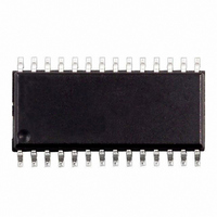
ST72F264G2M6 STMicroelectronics, ST72F264G2M6 Datasheet - Page 8

ST72F264G2M6
Manufacturer Part Number
ST72F264G2M6
Description
IC MCU 8BIT 8K 28 SOIC
Manufacturer
STMicroelectronics
Series
ST7r
Datasheet
1.STEVAL-ISQ002V1.pdf
(172 pages)
Specifications of ST72F264G2M6
Core Processor
ST7
Core Size
8-Bit
Speed
16MHz
Connectivity
I²C, SCI, SPI
Peripherals
LVD, POR, PWM, WDT
Number Of I /o
22
Program Memory Size
8KB (8K x 8)
Program Memory Type
FLASH
Ram Size
256 x 8
Voltage - Supply (vcc/vdd)
2.7 V ~ 5.5 V
Data Converters
A/D 6x10b
Oscillator Type
Internal
Operating Temperature
-40°C ~ 85°C
Package / Case
28-SOIC (7.5mm Width)
Processor Series
ST72F2x
Core
ST7
Data Bus Width
8 bit
Data Ram Size
256 B
Interface Type
I2C/SCI/SPI
Maximum Clock Frequency
8 MHz
Number Of Programmable I/os
22
Number Of Timers
3
Operating Supply Voltage
2.7 V to 5.5 V
Maximum Operating Temperature
+ 85 C
Mounting Style
SMD/SMT
Development Tools By Supplier
ST7F264-IND/USB, ST72F34X-SK/RAIS, ST7MDT10-DVP3, ST7MDT10-EMU3, STX-RLINK
Minimum Operating Temperature
- 40 C
On-chip Adc
6-ch x 10-bit
Controller Family/series
ST7
No. Of I/o's
22
Ram Memory Size
256Byte
Cpu Speed
8MHz
No. Of Timers
2
Embedded Interface Type
I2C, SCI, SPI
Rohs Compliant
Yes
For Use With
497-6423 - BOARD EVAL BASED ON ST72264G1497-5046 - KIT TOOL FOR ST7/UPSD/STR7 MCU
Lead Free Status / RoHS Status
Lead free / RoHS Compliant
Eeprom Size
-
Lead Free Status / Rohs Status
Lead free / RoHS Compliant
Other names
497-2106-5
Available stocks
Company
Part Number
Manufacturer
Quantity
Price
Company:
Part Number:
ST72F264G2M6
Manufacturer:
SCS
Quantity:
1 225
Part Number:
ST72F264G2M6
Manufacturer:
ST
Quantity:
20 000
ST72260Gx, ST72262Gx, ST72264Gx
PIN DESCRIPTION (Cont’d)
For external pin connection guidelines, refer to
126.
Legend / Abbreviations for
Type:
Input level:
In/Output level: C
Output level:
Port and control configuration:
Refer to
The RESET configuration of each pin is shown in bold. This configuration is valid as long as the device is
in reset state.
Table 1. Device Pin Description
8/172
– Input:
– Output:
10
11
12 10 E1 PB1 /OCMP1_A
13 11 F1 PB0 /ICAP1_A
14 12 F2 PC5/EXTCLK_A/AIN5 I/O
1
2
3
4
5
6
7
8
9
Pin n°
1
2
3
4
5
6
7
8
9
Section 9 "I/O PORTS" on page 38
C4 OSC1
C1 NC
C2 NC
D1 NC
C3 PB3/OCMP2_A
D2 PB2/ICAP2_A
A3 RESET
B3 OSC2
A2 PB7/SS
A1 PB6/SCK
B1 PB5/MISO
B2 PB4/MOSI
I = input, O = output, S = supply
A = Dedicated analog input
HS = 20 mA high sink (on N-buffer only)
float = floating, wpu = weak pull-up, int = interrupt
OD = open drain
Pin Name
T
3)
3)
= CMOS 0.3 V
Table
2)
DD
I/O C
I/O
I/O
I/O
I/O
I/O
I/O
I/O
I/O
O
I
1:
, PP = push-pull
/0.7 V
Level
T
C
C
C
C
C
C
C
C
C
T
T
T
T
T
T
T
T
T
DD
for more details on the software configuration of the I/O ports.
with input trigger
Section 13 "ELECTRICAL CHARACTERISTICS" on page
X
X
X
X
X
X
X
X
X ei0/ei1 X
Port / Control
Input
X
ei1
ei1
ei1
ei1
ei1
ei1
ei1
ei1
Output
X
X
X
X
X
X
X
X
X
X
Not Connected
X
X
X
X
X
X
X
X
X
1)
, ana = analog
Function
Top priority non maskable interrupt (ac-
tive low)
External clock input or Resonator oscilla-
tor inverter input or resistor input for RC
oscillator
Resonator oscillator inverter output or ca-
pacitor input for RC oscillator
Port B7
Port B6
Port B5
Port B4
Port B3
Port B2
Port B1
Port B0
Port C5
reset)
(after
Main
SPI Slave Select (active low)
SPI Serial Clock
SPI Master In/ Slave Out Data
SPI Master Out / Slave In Data
Timer A Output Compare 2
Timer A Input Capture 2
Timer A Output Compare 1
Caution: Negative current
injection not allowed on
this pin
Timer A Input Capture 1
Caution: Negative current
injection not allowed on
this pin
Timer A Input Clock or ADC
Analog Input 5
Alternate Function
4)
4)
.
.


