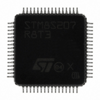
STM8S207R8T3 STMicroelectronics, STM8S207R8T3 Datasheet - Page 84

STM8S207R8T3
Manufacturer Part Number
STM8S207R8T3
Description
MCU 8BIT 64K MEMORY 64-LQFP
Manufacturer
STMicroelectronics
Series
STM8Sr
Datasheet
1.STEVAL-MKI030V1.pdf
(105 pages)
Specifications of STM8S207R8T3
Core Processor
STM8
Core Size
8-Bit
Speed
24MHz
Connectivity
I²C, IrDA, LIN, SPI, UART/USART
Peripherals
Brown-out Detect/Reset, POR, PWM, WDT
Number Of I /o
52
Program Memory Size
64KB (64K x 8)
Program Memory Type
FLASH
Eeprom Size
1.5K x 8
Ram Size
4K x 8
Voltage - Supply (vcc/vdd)
2.95 V ~ 5.5 V
Data Converters
A/D 16x10b
Oscillator Type
Internal
Operating Temperature
-40°C ~ 125°C
Package / Case
64-LQFP
Processor Series
STM8S20x
Core
STM8
Data Bus Width
8 bit
Data Ram Size
4 KB
Interface Type
I2C, SPI, UART
Maximum Clock Frequency
24 MHz
Number Of Programmable I/os
52
Number Of Timers
9
Maximum Operating Temperature
+ 125 C
Mounting Style
SMD/SMT
3rd Party Development Tools
EWSTM8
Development Tools By Supplier
STICE-SYS001
Minimum Operating Temperature
- 40 C
On-chip Adc
10 bit, 16 Channel
A/d Bit Size
10 bit
A/d Channels Available
16
Height
1.4 mm
Length
10 mm
Supply Voltage (max)
5.5 V
Supply Voltage (min)
2.95 V
Width
10 mm
For Use With
497-10032 - EVAL KIT MOTOR CONTROL STM8S497-10031 - EVAL KIT TOUCH SENSING STM8S497-10592 - BOARD DAUGHTER FOR STM8S207/8497-10593 - KIT STARTER FOR STM8S207/8 SER497-8506 - BOARD EVAL FOR STM8S
Lead Free Status / RoHS Status
Lead free / RoHS Compliant
Other names
497-8941
Available stocks
Company
Part Number
Manufacturer
Quantity
Price
Company:
Part Number:
STM8S207R8T3
Manufacturer:
NS
Quantity:
540
Company:
Part Number:
STM8S207R8T3
Manufacturer:
STMicroelectronics
Quantity:
10 000
Company:
Part Number:
STM8S207R8T3TR
Manufacturer:
STMicroelectronics
Quantity:
10 000
Electrical characteristics
10.3.10
84/105
10-bit ADC characteristics
Subject to general operating conditions for V
specified.
Table 44.
1. Data guaranteed by design, not tested in production..
2. During the sample time the input capacitance C
Symbol
V
t
V
V
C
t
f
CONV
V
t
STAB
ADC
REF+
source. The internal resistance of the analog source must allow the capacitance to reach its final voltage
level within t
the conversion result. Values for the sample clock t
REF-
S
DDA
ADC
AIN
(2)
ADC clock frequency
Analog supply
Positive reference voltage
Negative reference voltage
Conversion voltage range
Internal sample and hold
capacitor
Sampling time
Wakeup time from standby
Total conversion time (including
sampling time, 10-bit resolution)
ADC characteristics
S.
After the end of the sample time t
Parameter
Doc ID 14733 Rev 11
(2)
Devices with external
AIN
S
V
, changes of the analog input voltage have no effect on
V
V
DDA
S
(3 pF max) can be charged/discharged by the external
DDA
REF+
DDA
f
f
f
f
ADC
ADC
ADC
ADC
depend on programming.
Conditions
= 4.5 to 5.5 V
= 3 to 5.5 V
, f
/V
= 4 MHz
= 6 MHz
= 4 MHz
= 6 MHz
MASTER
REF-
pins
, and T
2.75
V
STM8S207xx, STM8S208xx
V
V
Min
REF-
SSA
SSA
A
1
1
3
(1)
unless otherwise
0.75
2.33
Typ
0.5
3.5
14
3
7
V
0.5
V
V
Max
REF+
5.5
DDA
DDA
4
6
(1)
1/f
MHz
Unit
pF
µs
µs
µs
µs
V
V
V
V
V
ADC


