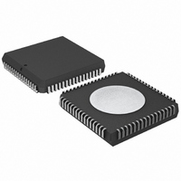
P87C554SFAA,512 NXP Semiconductors, P87C554SFAA,512 Datasheet - Page 28

P87C554SFAA,512
Manufacturer Part Number
P87C554SFAA,512
Description
IC 80C51 MCU 16K OTP 64-PLCC
Manufacturer
NXP Semiconductors
Series
87Cr
Specifications of P87C554SFAA,512
Core Processor
8051
Core Size
8-Bit
Speed
16MHz
Connectivity
EBI/EMI, I²C, UART/USART
Peripherals
POR, PWM, WDT
Number Of I /o
40
Program Memory Size
16KB (16K x 8)
Program Memory Type
OTP
Ram Size
512 x 8
Voltage - Supply (vcc/vdd)
2.7 V ~ 5.5 V
Data Converters
A/D 8x10b
Oscillator Type
Internal
Operating Temperature
-40°C ~ 85°C
Package / Case
68-PLCC
Cpu Family
87C
Device Core
80C51
Device Core Size
8b
Frequency (max)
16MHz
Interface Type
I2C/UART
Total Internal Ram Size
512Byte
# I/os (max)
40
Number Of Timers - General Purpose
3
Operating Supply Voltage (typ)
5V
Operating Supply Voltage (max)
5.5V
Operating Supply Voltage (min)
4.5V
On-chip Adc
7-chx10-bit
Instruction Set Architecture
CISC
Operating Temp Range
-40C to 85C
Operating Temperature Classification
Industrial
Mounting
Surface Mount
Pin Count
68
Package Type
PLCC
Processor Series
P87C5x
Core
80C51
Data Bus Width
8 bit
Data Ram Size
512 B
Maximum Clock Frequency
16 MHz
Number Of Programmable I/os
40
Number Of Timers
3
Operating Supply Voltage
2.7 V to 5.5 V
Maximum Operating Temperature
+ 85 C
Mounting Style
SMD/SMT
3rd Party Development Tools
PK51, CA51, A51, ULINK2
Minimum Operating Temperature
- 40 C
Package
68PLCC
Family Name
87C
Maximum Speed
16 MHz
Lead Free Status / RoHS Status
Lead free / RoHS Compliant
Eeprom Size
-
Lead Free Status / Rohs Status
Compliant
Other names
568-1255-5
935263922512
P87C554SFAA
935263922512
P87C554SFAA
Available stocks
Company
Part Number
Manufacturer
Quantity
Price
Company:
Part Number:
P87C554SFAA,512
Manufacturer:
Maxim
Quantity:
145
Company:
Part Number:
P87C554SFAA,512
Manufacturer:
NXP Semiconductors
Quantity:
10 000
between AVref+ and AVref–. If the analog input voltage range is from
Philips Semiconductors
10-Bit ADC Resolution and Analog Supply: Figure 24 shows how
the ADC is realized. The ADC has its own supply pins (AV
AV
DAC’s resistance-ladder. The ladder has 1023 equally spaced taps,
separated by a resistance of “R”. The first tap is located 0.5 x R
above Vref–, and the last tap is located 1.5 x R below Vref+. This
gives a total ladder resistance of 1024 x R. This structure ensures
that the DAC is monotonic and results in a symmetrical quantization
error as shown in Figure 26.
For input voltages between Vref– and (Vref–) + 1/2 LSB, the 10-bit
result of an A/D conversion will be 00 0000 0000B = 000H. For input
voltages between (Vref+) – 3/2 LSB and Vref+, the result of a
conversion will be 11 1111 1111B = 3FFH. AVref+ and AVref– may
be between AV
positive with respect to AVref–, and the input voltage (Vin) should be
2 V to 4 V, then 10-bit resolution can be obtained over this range if
AVref+ = 4V and AVref– = 2 V.
The result can always be calculated from the following formula:
2002 Mar 25
80C51 8-bit microcontroller – 12 clock operation
16K/512 OTP/RAM, 8 channel 10-bit A/D, I
capture/compare, high I/O
SS
Result + 1024
TOTAL RESISTANCE
=
=
) and two pins (Vref+ and Vref–) connected to each end of the
1023R + 2 x R/
1024R
DD
+ 0.2 V and AV
R/2
R
R
R
R
R
R/2
AV
V
ref)
IN
* AV
AV
AV
* AV
ref+
ref–
ref*
SS
ref*
– 0.2 V. AVref+ should be
Value 0000 0000 00
Value 1111 1111 11
V
V
ref
in
Figure 24. ADC Realization
DD
COMPARATOR
and
–
+
2
is output for voltages V
is output for voltages (V
C, PWM,
1023
1022
1021
3
2
1
0
DECODER
26
Power Reduction Modes
The P87C554 has two reduced power modes of operation: the idle
mode and the power-down mode. These modes are entered by
setting bits in the PCON special function register. When the
P87C554 enters the idle mode, the following functions are disabled:
CPU
Timer T2
PWM0, PWM1
ADC
In idle mode, the following functions remain active:
Timer 0
Timer 1
Timer T3
SIO0 SIO1
External interrupts
When the P87C554 enters the power-down mode, the oscillator is
stopped. The power-down mode is entered by setting the PD bit in
the PCON register. The PD bit can only be set if the EW input is tied
HIGH.
ref–
ref+
to (V
APPROXIMATION
– 3/2 LSB) to V
SUCCESSIVE
REGISTER
ref–
MSB
LSB
+ 1/2 LSB)
(halted)
(halted and reset)
(reset; outputs are high)
(may be enabled for operation in Idle mode
by setting bit AIDC (AUXR1.6) ).
ref+
APPROXIMATION
CONTROL LOGIC
SUCCESSIVE
P87C554
Product data
SU00961
START
READY


