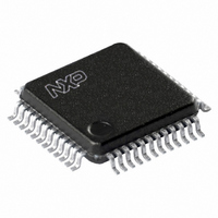
LPC2106FBD48/01,15 NXP Semiconductors, LPC2106FBD48/01,15 Datasheet - Page 22

LPC2106FBD48/01,15
Manufacturer Part Number
LPC2106FBD48/01,15
Description
IC ARM7 MCU FLASH 128K 48-LQFP
Manufacturer
NXP Semiconductors
Series
LPC2100r
Datasheet
1.LPC2104FBD480115.pdf
(41 pages)
Specifications of LPC2106FBD48/01,15
Program Memory Type
FLASH
Program Memory Size
128KB (128K x 8)
Package / Case
48-LQFP
Core Processor
ARM7
Core Size
16/32-Bit
Speed
60MHz
Connectivity
I²C, Microwire, SPI, SSI, SSP, UART/USART
Peripherals
POR, PWM, WDT
Number Of I /o
32
Ram Size
64K x 8
Voltage - Supply (vcc/vdd)
1.65 V ~ 3.6 V
Oscillator Type
Internal
Operating Temperature
-40°C ~ 85°C
Processor Series
LPC21
Core
ARM7TDMI-S
Data Bus Width
16 bit, 32 bit
Data Ram Size
64 KB
Interface Type
I2C/SPI/UART
Maximum Clock Frequency
60 MHz
Number Of Programmable I/os
32
Number Of Timers
2
Maximum Operating Temperature
+ 85 C
Mounting Style
SMD/SMT
3rd Party Development Tools
MDK-ARM, RL-ARM, ULINK2, KSK-LPC2106-PL, DB-LQFP48-LPC2106
Minimum Operating Temperature
- 40 C
Cpu Family
LPC2000
Device Core
ARM7TDMI-S
Device Core Size
16/32Bit
Frequency (max)
60MHz
Total Internal Ram Size
64KB
# I/os (max)
32
Number Of Timers - General Purpose
2
Operating Supply Voltage (typ)
1.8/3.3V
Operating Supply Voltage (max)
1.95/3.6V
Operating Supply Voltage (min)
1.65/3V
Instruction Set Architecture
RISC
Operating Temp Range
-40C to 85C
Operating Temperature Classification
Industrial
Mounting
Surface Mount
Pin Count
48
Package Type
LQFP
Lead Free Status / RoHS Status
Lead free / RoHS Compliant
For Use With
568-4310 - EVAL BOARD LPC2158 W/LCD568-4297 - BOARD EVAL LPC21XX MCB2100622-1019 - BOARD FOR LPC2106 48-LQFP622-1008 - BOARD FOR LPC9103 10-HVSON622-1005 - USB IN-CIRCUIT PROG ARM7 LPC2K568-1756 - BOARD EVAL FOR LPC210X ARM MCU
Eeprom Size
-
Data Converters
-
Lead Free Status / Rohs Status
Lead free / RoHS Compliant
Other names
568-4367
935286617151
LPC2106FBD48/01-S
935286617151
LPC2106FBD48/01-S
Available stocks
Company
Part Number
Manufacturer
Quantity
Price
Company:
Part Number:
LPC2106FBD48/01,15
Manufacturer:
NXP
Quantity:
250
Company:
Part Number:
LPC2106FBD48/01,15
Manufacturer:
NXP Semiconductors
Quantity:
10 000
NXP Semiconductors
LPC2104_2105_2106_7
Product data sheet
6.18.3 Reset and wake-up timer
6.18.4 Code security (Code Read Protection - CRP)
by 2, 4, 8, or 16 to produce the output clock. Since the minimum output divider value is 2,
it is insured that the PLL output has a 50 % duty cycle.The PLL is turned off and bypassed
following a chip Reset and may be enabled by software. The program must configure and
activate the PLL, wait for the PLL to Lock, then connect to the PLL as a clock source. The
PLL settling time is 100 s.
Reset has two sources on the LPC2104/2105/2106: the RESET pin and Watchdog Reset.
The RESET pin is a Schmitt trigger input pin with an additional glitch filter. Assertion of
chip Reset by any source starts the wake-up timer (see wake-up timer description below),
causing the internal chip reset to remain asserted until the external Reset is de-asserted,
the oscillator is running, a fixed number of clocks have passed, and the on-chip flash
controller has completed its initialization.
When the internal Reset is removed, the processor begins executing at address 0, which
is the Reset vector. At that point, all of the processor and peripheral registers have been
initialized to predetermined values.
The wake-up timer ensures that the oscillator and other analog functions required for chip
operation are fully functional before the processor is allowed to execute instructions. This
is important at power on, all types of Reset, and whenever any of the aforementioned
functions are turned off for any reason. Since the oscillator and other functions are turned
off during Power-down mode, any wake-up of the processor from Power-down mode
makes use of the wake-up timer.
The wake-up timer monitors the crystal oscillator as the means of checking whether it is
safe to begin code execution. When power is applied to the chip, or some event caused
the chip to exit Power-down mode, some time is required for the oscillator to produce a
signal of sufficient amplitude to drive the clock logic. The amount of time depends on
many factors, including the rate of V
and its electrical characteristics (if a quartz crystal is used), as well as any other external
circuitry (e.g. capacitors), and the characteristics of the oscillator itself under the existing
ambient conditions.
This feature of the LPC2104/2105/2106/01 allows the user to enable different levels of
security in the system so that access to the on-chip flash and use of the JTAG and ISP
can be restricted. When needed, CRP is invoked by programming a specific pattern into a
dedicated flash location. IAP commands are not affected by the CRP.
There are three levels of the Code Read Protection:
1. CRP1 disables access to the chip via the JTAG and allows partial flash update
2. CRP2 disables access to the chip via the JTAG and only allows full flash erase and
(excluding flash sector 0) using a limited set of the ISP commands. This mode is
useful when CRP is required and flash field updates are needed but all sectors can
not be erased.
update using a reduced set of the ISP commands.
Rev. 07 — 20 June 2008
DD
ramp (in the case of power on), the type of crystal
LPC2104/2105/2106
Single-chip 32-bit microcontrollers
© NXP B.V. 2008. All rights reserved.
22 of 41


