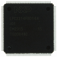
LPC2214FBD144/01,5 NXP Semiconductors, LPC2214FBD144/01,5 Datasheet - Page 10

LPC2214FBD144/01,5
Manufacturer Part Number
LPC2214FBD144/01,5
Description
IC ARM7 MCU FLASH 256K 144-LQFP
Manufacturer
NXP Semiconductors
Series
LPC2200r
Datasheet
1.LPC2212FBD144015.pdf
(45 pages)
Specifications of LPC2214FBD144/01,5
Program Memory Type
FLASH
Program Memory Size
256KB (256K x 8)
Package / Case
144-LQFP
Core Processor
ARM7
Core Size
16/32-Bit
Speed
60MHz
Connectivity
EBI/EMI, I²C, Microwire, SPI, SSI, SSP, UART/USART
Peripherals
POR, PWM, WDT
Number Of I /o
112
Ram Size
16K x 8
Voltage - Supply (vcc/vdd)
1.65 V ~ 1.95 V
Data Converters
A/D 8x10b
Oscillator Type
Internal
Operating Temperature
-40°C ~ 85°C
Processor Series
LPC22
Core
ARM7TDMI-S
Data Bus Width
16 bit, 32 bit
Data Ram Size
16 KB
Interface Type
I2C/JTAG/SPI/SSP/UART
Maximum Clock Frequency
60 MHz
Number Of Programmable I/os
112
Number Of Timers
2
Operating Supply Voltage
3.3 V
Maximum Operating Temperature
+ 85 C
Mounting Style
SMD/SMT
3rd Party Development Tools
MDK-ARM, RL-ARM, ULINK2
Minimum Operating Temperature
- 40 C
On-chip Adc
8-ch x 10-bit
Cpu Family
LPC2000
Device Core
ARM7TDMI-S
Device Core Size
16/32Bit
Frequency (max)
60MHz
Total Internal Ram Size
16KB
# I/os (max)
112
Number Of Timers - General Purpose
2
Operating Supply Voltage (typ)
1.8/3.3V
Operating Supply Voltage (max)
1.95/3.6V
Operating Supply Voltage (min)
1.65/2.5/3V
Instruction Set Architecture
RISC
Operating Temp Range
-40C to 85C
Operating Temperature Classification
Industrial
Mounting
Surface Mount
Pin Count
144
Package Type
LQFP
Lead Free Status / RoHS Status
Lead free / RoHS Compliant
For Use With
OM10091 - KIT DEV PHYCORE-ARM7/LPC2220622-1005 - USB IN-CIRCUIT PROG ARM7 LPC2K568-1757 - BOARD EVAL FOR LPC220X ARM MCU
Eeprom Size
-
Lead Free Status / Rohs Status
Lead free / RoHS Compliant
Other names
568-4318
935284893551
LPC2214FBD144/01-S
LPC2214FBD144/01-S
935284893551
LPC2214FBD144/01-S
LPC2214FBD144/01-S
Available stocks
Company
Part Number
Manufacturer
Quantity
Price
Company:
Part Number:
LPC2214FBD144/01,5
Manufacturer:
Intersil
Quantity:
637
Company:
Part Number:
LPC2214FBD144/01,5
Manufacturer:
NXP Semiconductors
Quantity:
10 000
Part Number:
LPC2214FBD144/01,5
Manufacturer:
NXP/恩智浦
Quantity:
20 000
NXP Semiconductors
Table 3.
LPC2212_2214_4
Product data sheet
Symbol
P3[3]/A3
P3[4]/A4
P3[5]/A5
P3[6]/A6
P3[7]/A7
P3[8]/A8
P3[9]/A9
P3[10]/A10
P3[11]/A11
P3[12]/A12
P3[13]/A13
P3[14]/A14
P3[15]/A15
P3[16]/A16
P3[17]/A17
P3[18]/A18
P3[19]/A19
P3[20]/A20
P3[21]/A21
P3[22]/A22
P3[23]/A23/XCLK
P3[24]/CS3
P3[25]/CS2
P3[26]/CS1
P3[27]/WE
P3[28]/BLS3/AIN7
P3[29]/BLS2/AIN6
P3[30]/BLS1
P3[31]/BLS0
n.c.
RESET
XTAL1
XTAL2
Pin description
Pin
81
80
74
73
72
71
66
65
64
63
62
56
55
53
48
47
46
45
44
41
40
36
35
30
29
28
27
97
96
22
135
142
141
…continued
Type Description
O
O
O
O
O
O
O
O
O
O
O
O
O
O
O
O
O
O
O
O
O
O
O
O
O
O
O
I
O
I
O
O
I
I
O
External memory address line 3.
External memory address line 4.
External memory address line 5.
External memory address line 6.
External memory address line 7.
External memory address line 8.
External memory address line 9.
External memory address line 10.
External memory address line 11.
External memory address line 12.
External memory address line 13.
External memory address line 14.
External memory address line 15.
External memory address line 16.
External memory address line 17.
External memory address line 18.
External memory address line 19.
External memory address line 20.
External memory address line 21.
External memory address line 22.
A23 — External memory address line 23.
XCLK — Clock output.
LOW-active Chip Select 3 signal.
(Bank 3 addresses range 0x8300 0000 to 0x83FF FFFF)
LOW-active Chip Select 2 signal.
(Bank 2 addresses range 0x8200 0000 to 0x82FF FFFF)
LOW-active Chip Select 1 signal.
(Bank 1 addresses range 0x8100 0000 to 0x81FF FFFF)
LOW-active Write enable signal.
BLS3 — LOW-active Byte Lane Select signal (Bank 3).
AIN7 — ADC, input 7. This analog input is always connected to its pin.
BLS2 — LOW-active Byte Lane Select signal (Bank 2).
AIN6 — ADC, input 6. This analog input is always connected to its pin.
LOW-active Byte Lane Select signal (Bank 1).
LOW-active Byte Lane Select signal (Bank 0).
Pin not connected.
external reset input; a LOW on this pin resets the device, causing I/O ports
and peripherals to take on their default states, and processor execution to
begin at address 0. TTL with hysteresis, 5 V tolerant.
input to the oscillator circuit and internal clock generator circuits.
output from the oscillator amplifier.
Rev. 04 — 3 January 2008
16/32-bit ARM microcontrollers
LPC2212/2214
© NXP B.V. 2008. All rights reserved.
10 of 45


