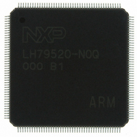
LH79520N0Q000B1;55 NXP Semiconductors, LH79520N0Q000B1;55 Datasheet - Page 31

LH79520N0Q000B1;55
Manufacturer Part Number
LH79520N0Q000B1;55
Description
IC ARM7 BLUESTREAK MCU 176LQFP
Manufacturer
NXP Semiconductors
Series
BlueStreak ; LH7r
Datasheet
1.LH79520N0Q000B155.pdf
(59 pages)
Specifications of LH79520N0Q000B1;55
Package / Case
176-LQFP
Core Processor
ARM7
Core Size
32-Bit
Speed
77.4MHz
Connectivity
EBI/EMI, IrDA, Microwire, SPI, SSI, SSP, UART/USART
Peripherals
DMA, LCD, POR, PWM, WDT
Number Of I /o
64
Program Memory Type
ROMless
Ram Size
32K x 8
Voltage - Supply (vcc/vdd)
1.62 V ~ 3.6 V
Oscillator Type
External
Operating Temperature
-40°C ~ 85°C
Processor Series
LH795
Core
ARM7TDMI-S
Data Bus Width
32 bit
Data Ram Size
32 KB
Interface Type
JTAG, UART
Maximum Clock Frequency
77.4 MHz
Number Of Programmable I/os
64
Number Of Timers
3
Operating Supply Voltage
1.8 V
Maximum Operating Temperature
+ 85 C
Mounting Style
SMD/SMT
3rd Party Development Tools
MDK-ARM, RL-ARM, ULINK2
Minimum Operating Temperature
- 40 C
Lead Free Status / RoHS Status
Lead free / RoHS Compliant
Eeprom Size
-
Program Memory Size
-
Data Converters
-
Lead Free Status / Rohs Status
Lead free / RoHS Compliant
Other names
568-4331
935285044557
LH79520N0Q000B1
935285044557
LH79520N0Q000B1
System-on-Chip
Static Memory Controller Waveforms
nWAIT INPUT
nWAIT input that can be used by an external device to
extend the wait time during a memory access. The
SMC samples nWAIT at the beginning of at the begin-
ning of each system clock cycle. The system clock
cycle in which the nCSx signal is asserted counts as
the first wait state. See Figure 11.
clock cycles after it has been asserted. To assure that
the current access (read or write) will be extended by
nWAIT, at least two wait states must be programmed
for this bank of memory. If N wait states are pro-
grammed, then the Static Memory Controller (SMC)
holds this state for N system clocks, or until the SMC
detects that nWAIT is inactive, whichever occurs last.
As the number of wait states programmed increases,
the amount of delay before nWAIT must be asserted
also increases. If only 2 wait states are programmed,
Preliminary data sheet
The Static Memory Controller (SMC) supports an
The SMC recognizes that nWAIT is active within 2
Rev. 01 — 16 July 2007
NXP Semiconductors
then nWAIT must be asserted in the clock cycle imme-
diately following the clock cycle during which the nCSx
signal is asserted. Once the SMC detects that the
external device has deactivated nWAIT, the SMC will
complete its access in 3 system clock cycles.
ing nCSx and asserting nWAIT is:
READ AND WRITE WAVEFORMS
External Static Memory Write. Figure 13 shows the
waveform and timing for an External Static Memory
Read, with one Wait State. Figure 14 shows the wave-
form and timing for an External Static Memory Read,
with two Wait States.
measurements are made from the Address Valid point
and HCLK is an internal signal, shown for reference only.
The formula for the allowable delay between assert-
tASSERT = (system clock period) × (Wait States - 1)
(where Wait States is from 2 to 31.)
Figure 12 shows the waveform and timing for an
The signal tIDD is shown without a setup time, as
LH79520
31


