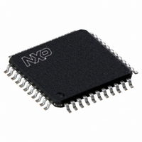
P89LV51RD2BBC,557 NXP Semiconductors, P89LV51RD2BBC,557 Datasheet - Page 18

P89LV51RD2BBC,557
Manufacturer Part Number
P89LV51RD2BBC,557
Description
IC 80C51 MCU FLASH 64K 44-TQFP
Manufacturer
NXP Semiconductors
Series
89LVr
Datasheet
1.P89LV51RD2BBC557.pdf
(76 pages)
Specifications of P89LV51RD2BBC,557
Program Memory Type
FLASH
Program Memory Size
64KB (64K x 8)
Package / Case
44-TQFP, 44-VQFP
Core Processor
8051
Core Size
8-Bit
Speed
33MHz
Connectivity
SPI, UART/USART
Peripherals
Brown-out Detect/Reset, POR, PWM, WDT
Number Of I /o
32
Ram Size
1K x 8
Voltage - Supply (vcc/vdd)
2.7 V ~ 3.6 V
Oscillator Type
Internal
Operating Temperature
0°C ~ 70°C
Processor Series
P89LV5x
Core
80C51
Data Bus Width
8 bit
Data Ram Size
1 KB
Interface Type
SPI/UART
Maximum Clock Frequency
40 MHz
Number Of Programmable I/os
32
Number Of Timers
3
Operating Supply Voltage
2.7 V to 3.6 V
Maximum Operating Temperature
+ 70 C
Mounting Style
SMD/SMT
3rd Party Development Tools
PK51, CA51, A51, ULINK2
Minimum Operating Temperature
0 C
Cpu Family
89LV
Device Core
80C51
Device Core Size
8b
Frequency (max)
40MHz
Total Internal Ram Size
1KB
# I/os (max)
32
Number Of Timers - General Purpose
3
Operating Supply Voltage (typ)
3.3V
Operating Supply Voltage (max)
3.6V
Operating Supply Voltage (min)
2.7V
Instruction Set Architecture
CISC
Operating Temp Range
0C to 70C
Operating Temperature Classification
Commercial
Mounting
Surface Mount
Pin Count
44
Package Type
TQFP
Lead Free Status / RoHS Status
Lead free / RoHS Compliant
For Use With
622-1017 - BOARD 44-ZIF PLCC SOCKET622-1008 - BOARD FOR LPC9103 10-HVSON622-1001 - USB IN-CIRCUIT PROG 80C51ISP
Eeprom Size
-
Data Converters
-
Lead Free Status / Rohs Status
Lead free / RoHS Compliant
Other names
568-1289
935274177557
P89LV51RD2BBC
935274177557
P89LV51RD2BBC
Available stocks
Company
Part Number
Manufacturer
Quantity
Price
Company:
Part Number:
P89LV51RD2BBC,557
Manufacturer:
NXP Semiconductors
Quantity:
10 000
NXP Semiconductors
P89LV51RB2_RC2_RD2_5
Product data sheet
DPTR points to 0A0H and data in ‘A’ is written to address 0A0H of the expanded RAM
rather than external memory. Access to external memory higher than 2FFH using the
MOVX instruction will access external memory (0300H to FFFFH) and will perform in the
same way as the standard 8051, with P0 and P2 as data/address bus, and P3.6 and P3.7
as write and read timing signals.
When EXTRAM = 1, MOVX@Ri and MOVX@DPTR will be similar to the standard 8051.
Using MOVX @Ri provides an 8-bit address with multiplexed data on Port 0. Other output
port pins can be used to output higher order address bits. This provides external paging
capabilities. Using MOVX@DPTR generates a 16-bit address. This allows external
addressing up to 64 kB. Port 2 provides the high-order eight address bits (DPH), and
Port 0 multiplexes the low-order eight address bits (DPL) with data. Both MOVX@Ri and
MOVX@DPTR generates the necessary read and write signals (P3.6, - WR and P3.7, -
RD) for external memory use.
with EXTRAM bit.
The stack pointer (SP) can be located anywhere within the 256 B of internal RAM (lower
128 B and upper 128 B). The stack pointer may not be located in any part of the expanded
RAM.
Table 9.
[1]
Register AUXR
EXTRAM = 0
EXTRAM = 1
Access limited to Expanded RAM address within 0 to 0FFH; cannot access 100H to 02FFH.
External data memory RD, WR with EXTRAM bit
Rev. 05 — 15 December 2009
MOVX @DPTR, A or MOVX A, @DPTR
ADDR < 0300H
RD/WR not asserted
RD/WR asserted
Table 9
shows external data memory RD, WR operation
P89LV51RB2/RC2/RD2
ADDR
RD/WR asserted
RD/WR asserted
8-bit microcontrollers with 80C51 core
0300H
[1]
MOVX @Ri, A or
MOVX A, @Ri
ADDR = any
RD/WR not asserted
RD/WR asserted
© NXP B.V. 2009. All rights reserved.
18 of 76


