PIC12CE673/JW Microchip Technology, PIC12CE673/JW Datasheet - Page 73
PIC12CE673/JW
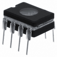
Manufacturer Part Number
PIC12CE673/JW
Description
IC MCU EPROM 1KX14 A/D&EE 8CDIP
Manufacturer
Microchip Technology
Series
PIC® 12Cr
Datasheets
1.PIC16F688T-ISL.pdf
(688 pages)
2.PIC12CE673-10P.pdf
(129 pages)
3.PIC12CE673-10P.pdf
(3 pages)
4.PIC12CE673-10P.pdf
(14 pages)
5.PIC12CE673-10P.pdf
(12 pages)
Specifications of PIC12CE673/JW
Core Processor
PIC
Core Size
8-Bit
Speed
10MHz
Peripherals
POR, WDT
Number Of I /o
5
Program Memory Size
1.75KB (1K x 14)
Program Memory Type
EPROM, UV
Eeprom Size
16 x 8
Ram Size
128 x 8
Voltage - Supply (vcc/vdd)
3 V ~ 5.5 V
Data Converters
A/D 4x8b
Oscillator Type
Internal
Operating Temperature
0°C ~ 70°C
Package / Case
8-CDIP (0.300", 7.62mm) Window
For Use With
ISPICR1 - ADAPTER IN-CIRCUIT PROGRAMMINGAC124001 - MODULE SKT PROMATEII 8DIP/SOIC
Lead Free Status / RoHS Status
Contains lead / RoHS non-compliant
Connectivity
-


4.2
1997 Microchip Technology Inc.
OSC2/CLKOUT
(RC mode)
Clocking Scheme/Instruction Cycle
OSC1
Q4
PC
Q2
Q3
Q1
The clock input (from OSC1) is internally divided by four to generate four non-overlapping
quadrature clocks, namely Q1, Q2, Q3, and Q4. Internally, the program counter (PC) is incre-
mented every Q1, and the instruction is fetched from the program memory and latched into the
instruction register in Q4. The instruction is decoded and executed during the following Q1
through Q4. The clocks and instruction execution flow are illustrated in
Example
Figure 4-3: Clock/Instruction Cycle
Q1
Execute INST (PC-1)
Fetch INST (PC)
Q2
T
4-1.
CY
PC
1
Q3
Q4
Q1
Execute INST (PC)
Fetch INST (PC+1)
Section 4. Architecture
Q2
T
PC+1
CY
2
Q3
Q4
Q1
Execute INST (PC+1)
Fetch INST (PC+2)
Q2
T
PC+2
CY
3
Q3
Q4
DS31004A-page 4-5
Figure
Internal
phase
clock
4-3, and
4
Related parts for PIC12CE673/JW
Image
Part Number
Description
Manufacturer
Datasheet
Request
R

Part Number:
Description:
8-Pin/ 8-Bit CMOS Microcontroller with EEPROM Data Memory
Manufacturer:
Microchip Technology
Part Number:
Description:
IC, 8BIT MCU, PIC12, 32MHZ, DFN-8
Manufacturer:
Microchip Technology
Datasheet:
Part Number:
Description:
IC, 8BIT MCU, PIC12, 32MHZ, DFN-8
Manufacturer:
Microchip Technology
Datasheet:

Part Number:
Description:
Manufacturer:
Microchip Technology Inc.
Datasheet:
Part Number:
Description:
Manufacturer:
Microchip Technology Inc.
Datasheet:
Part Number:
Description:
Manufacturer:
Microchip Technology Inc.
Datasheet:
Part Number:
Description:
Manufacturer:
Microchip Technology Inc.
Datasheet:
Part Number:
Description:
Manufacturer:
Microchip Technology Inc.
Datasheet:
Part Number:
Description:
Manufacturer:
Microchip Technology Inc.
Datasheet:
Part Number:
Description:
Manufacturer:
Microchip Technology Inc.
Datasheet: