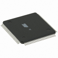
ATMEGA6450-16AU Atmel, ATMEGA6450-16AU Datasheet - Page 123

ATMEGA6450-16AU
Manufacturer Part Number
ATMEGA6450-16AU
Description
IC AVR MCU FLASH 64K 100TQFP
Manufacturer
Atmel
Series
AVR® ATmegar
Datasheet
1.ATMEGA325-16MU.pdf
(362 pages)
Specifications of ATMEGA6450-16AU
Core Processor
AVR
Core Size
8-Bit
Speed
16MHz
Connectivity
SPI, UART/USART, USI
Peripherals
Brown-out Detect/Reset, POR, PWM, WDT
Number Of I /o
68
Program Memory Size
64KB (32K x 16)
Program Memory Type
FLASH
Eeprom Size
2K x 8
Ram Size
4K x 8
Voltage - Supply (vcc/vdd)
2.7 V ~ 5.5 V
Data Converters
A/D 8x10b
Oscillator Type
Internal
Operating Temperature
-40°C ~ 85°C
Package / Case
100-TQFP, 100-VQFP
Processor Series
ATMEGA64x
Core
AVR8
Data Bus Width
8 bit
Data Ram Size
4 KB
Interface Type
SPI, UART, USI
Maximum Clock Frequency
16 MHz
Number Of Programmable I/os
69
Number Of Timers
3
Operating Supply Voltage
2.7 V to 5.5 V
Maximum Operating Temperature
+ 85 C
Mounting Style
SMD/SMT
Development Tools By Supplier
ATAVRDRAGON, ATSTK500, ATSTK600, ATAVRISP2, ATAVRONEKIT
Minimum Operating Temperature
- 40 C
On-chip Adc
10 bit, 8 Channel
Package
100TQFP
Device Core
AVR
Family Name
ATmega
Maximum Speed
16 MHz
For Use With
ATSTK600-TQFP100 - STK600 SOCKET/ADAPTER 100-TQFP770-1007 - ISP 4PORT ATMEL AVR MCU SPI/JTAG770-1005 - ISP 4PORT FOR ATMEL AVR MCU JTAG770-1004 - ISP 4PORT FOR ATMEL AVR MCU SPIATAVRISP2 - PROGRAMMER AVR IN SYSTEMATSTK504 - STARTER KIT AVR EXP MOD 100P LCD
Lead Free Status / RoHS Status
Lead free / RoHS Compliant
Available stocks
Company
Part Number
Manufacturer
Quantity
Price
Part Number:
ATMEGA6450-16AU
Manufacturer:
ATMEL/爱特梅尔
Quantity:
20 000
- Current page: 123 of 362
- Download datasheet (7Mb)
16.11 Register Description
16.11.1
2570M–AVR–04/11
TCCR1A – Timer/Counter1 Control Register A
Figure 16-13. Timer/Counter Timing Diagram, with Prescaler (f
• Bit 7:6 – COM1A1:0: Compare Output Mode for Unit A
• Bit 5:4 – COM1B1:0: Compare Output Mode for Unit B
The COM1A1:0 and COM1B1:0 control the Output Compare pins (OC1A and OC1B respec-
tively) behavior. If one or both of the COM1A1:0 bits are written to one, the OC1A output
overrides the normal port functionality of the I/O pin it is connected to. If one or both of the
COM1B1:0 bit are written to one, the OC1B output overrides the normal port functionality of the
I/O pin it is connected to. However, note that the Data Direction Register (DDR) bit correspond-
ing to the OC1A or OC1B pin must be set in order to enable the output driver.
When the OC1A or OC1B is connected to the pin, the function of the COM1x1:0 bits is depen-
dent of the WGM13:0 bits setting.
WGM13:0 bits are set to a Normal or a CTC mode (non-PWM).
Table 16-2.
Bit
(0x80)
Read/Write
Initial Value
COM1A1/COM1B1
and ICF n
(PC and PFC PWM)
TOVn
(CTC and FPWM)
(Update at TOP)
0
0
1
1
OCRnx
TCNTn
TCNTn
as TOP)
(clk
clk
clk
COM1A1
I/O
(FPWM)
I/O
Tn
/8)
R/W
(if used
Compare Output Mode, non-PWM
7
0
COM1A0
COM1A0/COM1B0
R/W
6
0
TOP - 1
TOP - 1
0
1
0
1
COM1B1
R/W
Old OCRnx Value
5
0
Table 16-2
COM1B0
R/W
4
0
Description
Normal port operation, OC1A/OC1B
disconnected.
Toggle OC1A/OC1B on Compare Match.
Clear OC1A/OC1B on Compare Match (Set
output to low level).
Set OC1A/OC1B on Compare Match (Set output
to high level).
ATmega325/3250/645/6450
shows the COM1x1:0 bit functionality when the
TOP
TOP
R
3
–
0
R
2
0
–
BOTTOM
TOP - 1
clk_I/O
WGM11
R/W
1
0
New OCRnx Value
/8)
WGM10
R/W
0
0
BOTTOM + 1
TOP - 2
TCCR1A
123
Related parts for ATMEGA6450-16AU
Image
Part Number
Description
Manufacturer
Datasheet
Request
R

Part Number:
Description:
Manufacturer:
Atmel Corporation
Datasheet:

Part Number:
Description:
IC AVR MCU FLASH 64K 64TQFP
Manufacturer:
Atmel
Datasheet:

Part Number:
Description:
IC AVR MCU FLASH 64K 5V 64TQFP
Manufacturer:
Atmel
Datasheet:

Part Number:
Description:
IC AVR MCU FLASH 64K 64-QFN
Manufacturer:
Atmel
Datasheet:

Part Number:
Description:
MCU AVR 64KB FLASH 16MHZ 64TQFP
Manufacturer:
Atmel
Datasheet:

Part Number:
Description:
MCU AVR 64KB FLASH 16MHZ 64QFN
Manufacturer:
Atmel
Datasheet:

Part Number:
Description:
IC AVR MCU FLASH 64K 5V 64QFN
Manufacturer:
Atmel
Datasheet:

Part Number:
Description:
Manufacturer:
Atmel Corporation
Datasheet:

Part Number:
Description:
Manufacturer:
ATMEL Corporation
Datasheet:

Part Number:
Description:
Manufacturer:
ATMEL Corporation
Datasheet:

Part Number:
Description:
IC AVR MCU 64K 16MHZ 5V 64TQFP
Manufacturer:
Atmel
Datasheet:

Part Number:
Description:
IC AVR MCU 64K 16MHZ 5V 64-QFN
Manufacturer:
Atmel
Datasheet:

Part Number:
Description:
IC AVR MCU 64K 16MHZ COM 64-TQFP
Manufacturer:
Atmel
Datasheet:

Part Number:
Description:
IC AVR MCU 64K 16MHZ IND 64-TQFP
Manufacturer:
Atmel
Datasheet:


