AT89C51CC02CA-RATUM Atmel, AT89C51CC02CA-RATUM Datasheet - Page 7
AT89C51CC02CA-RATUM
Manufacturer Part Number
AT89C51CC02CA-RATUM
Description
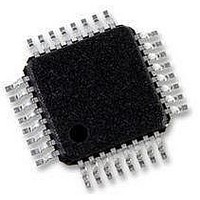
IC 8051 MCU FLASH 16K 32-VQFP
Manufacturer
Atmel
Series
AT89C CANr
Datasheet
1.T89C51CC02CA-TDSIM.pdf
(159 pages)
Specifications of AT89C51CC02CA-RATUM
Core Processor
8051
Core Size
8-Bit
Speed
40MHz
Connectivity
CAN, UART/USART
Peripherals
POR, PWM, WDT
Number Of I /o
20
Program Memory Size
16KB (16K x 8)
Program Memory Type
FLASH
Eeprom Size
2K x 8
Ram Size
512 x 8
Voltage - Supply (vcc/vdd)
3 V ~ 5.5 V
Data Converters
A/D 8x10b
Oscillator Type
External
Operating Temperature
-40°C ~ 85°C
Package / Case
32-TQFP, 32-VQFP
Processor Series
AT89x
Core
8051
Data Bus Width
8 bit
Data Ram Size
512 B
Interface Type
UART
Maximum Clock Frequency
40 MHz
Number Of Programmable I/os
20
Number Of Timers
1
Operating Supply Voltage
3 V to 5.5 V
Maximum Operating Temperature
+ 85 C
Mounting Style
SMD/SMT
3rd Party Development Tools
PK51, CA51, A51, ULINK2
Development Tools By Supplier
CANADAPT28
Minimum Operating Temperature
- 40 C
On-chip Adc
10 bit, 8 Channel
For Use With
AT89OCD-01 - USB EMULATOR FOR AT8XC51 MCU
Lead Free Status / RoHS Status
Lead free / RoHS Compliant
Available stocks
Company
Part Number
Manufacturer
Quantity
Price


I/O Configurations
Port Structure
4126L–CAN–01/08
Each Port SFR operates via type-D latches, as illustrated in Figure 1 for Ports 3 and 4. A
CPU ’write to latch’ signal initiates transfer of internal bus data into the type-D latch. A
CPU ’read latch’ signal transfers the latched Q output onto the internal bus. Similarly, a
’read pin’ signal transfers the logical level of the Port pin. Some Port data instructions
activate the ’read latch’ signal while others activate the ’read pin’ signal. Latch instruc-
tions are referred to as Read-Modify-Write instructions. Each I/O line may be
independently programmed as input or output.
Figure 1 shows the structure of Ports, which have internal pull-ups. An external source
can pull the pin low. Each Port pin can be configured either for general-purpose I/O or
for its alternate input output function.
To use a pin for general-purpose output, set or clear the corresponding bit in the Px reg-
ister (x = 1 to 4). To use a pin for general-purpose input, set the bit in the Px register.
This turns off the output FET drive.
To configure a pin for its alternate function, set the bit in the Px register. When the latch
is set, the ’alternate output function’ signal controls the output level (See Figure 1). The
operation of Ports is discussed further in ’Quasi-Bi-directional Port Operation’
paragraph.
Figure 1. Ports Structure
Note:
READ
LATCH
INTERNAL
BUS
WRITE
TO
LATCH
READ
PIN
1. The internal pull-up can be disabled on P1 when analog function is selected.
D
CL
LATCH
Q
ALTERNATE
OUTPUT
FUNCTION
ALTERNATE
INPUT
FUNCTION
AT/T89C51CC02
VCC
INTERNAL
PULL-UP (1)
P1.x
P2.x
P3.x
P4.x
(1)
7
Related parts for AT89C51CC02CA-RATUM
Image
Part Number
Description
Manufacturer
Datasheet
Request
R

Part Number:
Description:
Manufacturer:
Atmel Corporation
Datasheet:
Part Number:
Description:
At89c51cc02, T89c51cc02 Enhanced 8-bit Microcontroller With Can Controller And Flash
Manufacturer:
ATMEL Corporation
Datasheet:

Part Number:
Description:
DEV KIT FOR AVR/AVR32
Manufacturer:
Atmel
Datasheet:
Part Number:
Description:
INTERVAL AND WIPE/WASH WIPER CONTROL IC WITH DELAY
Manufacturer:
ATMEL Corporation
Datasheet:
Part Number:
Description:
Low-Voltage Voice-Switched IC for Hands-Free Operation
Manufacturer:
ATMEL Corporation
Datasheet:
Part Number:
Description:
MONOLITHIC INTEGRATED FEATUREPHONE CIRCUIT
Manufacturer:
ATMEL Corporation
Datasheet:
Part Number:
Description:
AM-FM Receiver IC U4255BM-M
Manufacturer:
ATMEL Corporation
Datasheet:
Part Number:
Description:
Monolithic Integrated Feature Phone Circuit
Manufacturer:
ATMEL Corporation
Datasheet:
Part Number:
Description:
Multistandard Video-IF and Quasi Parallel Sound Processing
Manufacturer:
ATMEL Corporation
Datasheet:
Part Number:
Description:
High-performance EE PLD
Manufacturer:
ATMEL Corporation
Datasheet:
Part Number:
Description:
8-bit Flash Microcontroller
Manufacturer:
ATMEL Corporation
Datasheet:
Part Number:
Description:
2-Wire Serial EEPROM
Manufacturer:
ATMEL Corporation
Datasheet: