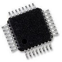
AT89C51CC02CA-RATUM Atmel, AT89C51CC02CA-RATUM Datasheet - Page 35

AT89C51CC02CA-RATUM
Manufacturer Part Number
AT89C51CC02CA-RATUM
Description
IC 8051 MCU FLASH 16K 32-VQFP
Manufacturer
Atmel
Series
AT89C CANr
Datasheet
1.T89C51CC02CA-TDSIM.pdf
(159 pages)
Specifications of AT89C51CC02CA-RATUM
Core Processor
8051
Core Size
8-Bit
Speed
40MHz
Connectivity
CAN, UART/USART
Peripherals
POR, PWM, WDT
Number Of I /o
20
Program Memory Size
16KB (16K x 8)
Program Memory Type
FLASH
Eeprom Size
2K x 8
Ram Size
512 x 8
Voltage - Supply (vcc/vdd)
3 V ~ 5.5 V
Data Converters
A/D 8x10b
Oscillator Type
External
Operating Temperature
-40°C ~ 85°C
Package / Case
32-TQFP, 32-VQFP
Processor Series
AT89x
Core
8051
Data Bus Width
8 bit
Data Ram Size
512 B
Interface Type
UART
Maximum Clock Frequency
40 MHz
Number Of Programmable I/os
20
Number Of Timers
1
Operating Supply Voltage
3 V to 5.5 V
Maximum Operating Temperature
+ 85 C
Mounting Style
SMD/SMT
3rd Party Development Tools
PK51, CA51, A51, ULINK2
Development Tools By Supplier
CANADAPT28
Minimum Operating Temperature
- 40 C
On-chip Adc
10 bit, 8 Channel
For Use With
AT89OCD-01 - USB EMULATOR FOR AT8XC51 MCU
Lead Free Status / RoHS Status
Lead free / RoHS Compliant
Available stocks
Company
Part Number
Manufacturer
Quantity
Price
FM0 Memory Architecture
User Space
Extra Row (XRow)
Hardware Security Byte
Column Latches
Cross Flash Memory Access
Description
4126L–CAN–01/08
The Flash memory is made up of 4 blocks (See Figure 13):
1. The memory array (user space) 16K Bytes
2. The Extra Row
3. The Hardware security bits
4. The column latch registers
This space is composed of a 16K Bytes Flash memory organized in 128 pages of 128
Bytes. It contains the user’s application code.
This row is a part of FM0 and has a size of 128 Bytes. The extra row may contain infor-
mation for boot loader usage.
The Hardware security Byte space is a part of FM0 and has a size of 1 byte.
The 4 MSB can be read/written by software, the 4 LSB can only be read by software and
written by hardware in parallel mode.
The column latches, also part of FM0, have a size of full page (128 Bytes).
The column latches are the entrance buffers of the three previous memory locations
(user array, XROW and Hardware security byte).
The FM0 memory can be programmed as describe on Table 21. Programming FM0
from FM0 is impossible.
The FM1 memory can be program only by parallel programming.
Table 21 show all software Flash access allowed.
Table 21. Cross Flash Memory Access
(user Flash)
(boot Flash)
FM0
FM1
Load column latch
Load column latch
Action
Read
Write
Read
Write
(user Flash)
FM0
ok
ok
ok
ok
ok
-
AT/T89C51CC02
(boot Flash)
FM1
ok
-
-
-
-
-
35


