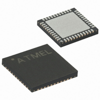
ATMEGA16-16MU Atmel, ATMEGA16-16MU Datasheet - Page 240

ATMEGA16-16MU
Manufacturer Part Number
ATMEGA16-16MU
Description
IC AVR MCU 16K 16MHZ 5V 44-QFN
Manufacturer
Atmel
Series
AVR® ATmegar
Specifications of ATMEGA16-16MU
Core Processor
AVR
Core Size
8-Bit
Speed
16MHz
Connectivity
I²C, SPI, UART/USART
Peripherals
Brown-out Detect/Reset, POR, PWM, WDT
Number Of I /o
32
Program Memory Size
16KB (8K x 16)
Program Memory Type
FLASH
Eeprom Size
512 x 8
Ram Size
1K x 8
Voltage - Supply (vcc/vdd)
4.5 V ~ 5.5 V
Data Converters
A/D 8x10b
Oscillator Type
Internal
Operating Temperature
-40°C ~ 85°C
Package / Case
44-VQFN Exposed Pad
Cpu Family
ATmega
Device Core
AVR
Device Core Size
8b
Frequency (max)
16MHz
Interface Type
JTAG/SPI/UART
Total Internal Ram Size
1KB
# I/os (max)
32
Number Of Timers - General Purpose
3
Operating Supply Voltage (typ)
5V
Operating Supply Voltage (max)
5.5V
Operating Supply Voltage (min)
4.5V
On-chip Adc
8-chx10-bit
Instruction Set Architecture
RISC
Operating Temp Range
-40C to 85C
Operating Temperature Classification
Industrial
Mounting
Surface Mount
Pin Count
44
Package Type
MLF
Processor Series
ATMEGA16x
Core
AVR8
Data Bus Width
8 bit
Data Ram Size
1 KB
Maximum Clock Frequency
16 MHz
Number Of Programmable I/os
32
Number Of Timers
3
Operating Supply Voltage
4.5 V to 5.5 V
Maximum Operating Temperature
+ 85 C
Mounting Style
SMD/SMT
3rd Party Development Tools
EWAVR, EWAVR-BL
Development Tools By Supplier
ATAVRDRAGON, ATSTK500, ATSTK600, ATAVRISP2, ATAVRONEKIT
Minimum Operating Temperature
- 40 C
Package
44MLF
Family Name
ATmega
Maximum Speed
16 MHz
Controller Family/series
AVR MEGA
No. Of I/o's
32
Eeprom Memory Size
512Byte
Ram Memory Size
1KB
Cpu Speed
16MHz
Rohs Compliant
Yes
For Use With
ATSTK600-TQFP44 - STK600 SOCKET/ADAPTER 44-TQFPATSTK600 - DEV KIT FOR AVR/AVR32770-1007 - ISP 4PORT ATMEL AVR MCU SPI/JTAGATAVRISP2 - PROGRAMMER AVR IN SYSTEMATJTAGICE2 - AVR ON-CHIP D-BUG SYSTEMATSTK500 - PROGRAMMER AVR STARTER KIT
Lead Free Status / RoHS Status
Lead free / RoHS Compliant
- Current page: 240 of 357
- Download datasheet (8Mb)
2466T–AVR–07/10
•
As an example, consider the task of verifying a 1.5V ±5% input signal at ADC channel 3 when
the power supply is 5.0V and AREF is externally connected to V
The recommended values from
in
“Actions” describes what JTAG instruction to be used before filling the Boundary-scan Register
with the succeeding columns. The verification should be done on the data scanned out when
scanning in the data on the same row in the table.
Table 93. Algorithm for Using the ADC
Using this algorithm, the timing constraint on the HOLD signal constrains the TCK clock fre-
quency. As the algorithm keeps HOLD high for five steps, the TCK clock frequency has to be at
least five times the number of scan bits divided by the maximum hold time, t
Step
10
11
Table
1
2
3
4
5
6
7
8
9
controlling/observing any ADC signal, or perform a dummy conversion before using the first
result.
The DAC values must be stable at the midpoint value 0x200 when having the HOLD signal
low (Sample mode).
Actions
SAMPLE
_PRELO
AD
EXTEST
Verify the
COMP bit
scanned
out to be
0
Verify the
COMP bit
scanned
out to be
1
93. Only the DAC and Port Pin values of the Scan-chain are shown. The column
The lower limit is:
The upper limit is:
ADCEN
1
1
1
1
1
1
1
1
1
1
1
DAC
0x200
0x200
0x200
0x123
0x123
0x200
0x200
0x200
0x143
0x143
0x200
Table 92
MUXEN
0x08
0x08
0x08
0x08
0x08
0x08
0x08
0x08
0x08
0x08
0x08
1024 1,5V 0,95 5V
1024 1,5V 1,05 5V
are used unless other values are given in the algorithm
⋅
⋅
HOLD
1
0
1
1
1
1
0
1
1
1
1
⋅
⋅
PRECH
⁄
⁄
1
1
1
1
0
1
1
1
1
0
1
=
=
291
323
PA3.
Data
CC
0
0
0
0
0
0
0
0
0
0
0
.
=
=
0x123
0x143
ATmega16(L)
PA3.
Control
0
0
0
0
0
0
0
0
0
0
0
hold,max
PA3.
Pullup_
Enable
.
0
0
0
0
0
0
0
0
0
0
0
240
Related parts for ATMEGA16-16MU
Image
Part Number
Description
Manufacturer
Datasheet
Request
R

Part Number:
Description:
Manufacturer:
Atmel Corporation
Datasheet:

Part Number:
Description:
IC AVR MCU 16K 16MHZ 5V 44TQFP
Manufacturer:
Atmel
Datasheet:

Part Number:
Description:
IC AVR MCU 16K 16MHZ 5V 40DIP
Manufacturer:
Atmel
Datasheet:

Part Number:
Description:
MCU AVR 16K FLASH 16MHZ 44-QFN
Manufacturer:
Atmel
Datasheet:

Part Number:
Description:
IC AVR MCU 16K 16MHZ COM 40-DIP
Manufacturer:
Atmel
Datasheet:

Part Number:
Description:
IC AVR MCU 16K 16MHZ COM 44-QFN
Manufacturer:
Atmel
Datasheet:

Part Number:
Description:
IC AVR MCU 16K 16MHZ IND 40-DIP
Manufacturer:
Atmel
Datasheet:

Part Number:
Description:
IC AVR MCU 16K 16MHZ IND 44-QFN
Manufacturer:
Atmel
Datasheet:

Part Number:
Description:
IC AVR MCU 16K 16MHZ IND 44-TQFP
Manufacturer:
Atmel
Datasheet:

Part Number:
Description:
IC MCU 8BIT 16KB FLASH 44TQFP
Manufacturer:
Atmel
Datasheet:

Part Number:
Description:
MCU AVR 16K FLASH 16MHZ 44-TQFP
Manufacturer:
Atmel
Datasheet:

Part Number:
Description:
IC AVR MCU 16K 16MHZ COM 44-TQFP
Manufacturer:
Atmel
Datasheet:

Part Number:
Description:
IC MCU AVR 16K 5V 16MHZ 44-TQFP
Manufacturer:
Atmel
Datasheet:


