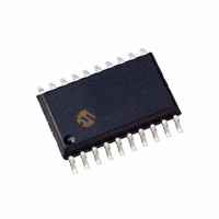
DSPIC33FJ12MC201-I/SO Microchip Technology, DSPIC33FJ12MC201-I/SO Datasheet - Page 121

DSPIC33FJ12MC201-I/SO
Manufacturer Part Number
DSPIC33FJ12MC201-I/SO
Description
IC DSPIC MCU/DSP 12K 20SOIC
Manufacturer
Microchip Technology
Series
dsPIC™ 33Fr
Datasheets
1.PIC24HJ12GP201-ISO.pdf
(84 pages)
2.DSPIC33FJ12MC201-ISO.pdf
(288 pages)
3.DSPIC33FJ12MC201-ISO.pdf
(14 pages)
4.DSPIC33FJ12MC201-IP.pdf
(284 pages)
Specifications of DSPIC33FJ12MC201-I/SO
Program Memory Type
FLASH
Program Memory Size
12KB (12K x 8)
Package / Case
20-SOIC (7.5mm Width)
Core Processor
dsPIC
Core Size
16-Bit
Speed
40 MIPs
Connectivity
I²C, IrDA, SPI, UART/USART
Peripherals
Brown-out Detect/Reset, Motor Control PWM, QEI, POR, PWM, WDT
Number Of I /o
15
Ram Size
1K x 8
Voltage - Supply (vcc/vdd)
3 V ~ 3.6 V
Data Converters
A/D 4x10b
Oscillator Type
Internal
Operating Temperature
-40°C ~ 85°C
Product
DSCs
Data Bus Width
16 bit
Processor Series
DSPIC33F
Core
dsPIC
Maximum Clock Frequency
40 MHz
Number Of Programmable I/os
15
Data Ram Size
1 KB
Maximum Operating Temperature
+ 85 C
Mounting Style
SMD/SMT
3rd Party Development Tools
52713-733, 52714-737, 53276-922, EWDSPIC
Development Tools By Supplier
PG164130, DV164035, DV244005, DV164005, PG164120, DM240001, DV164033
Minimum Operating Temperature
- 40 C
Lead Free Status / RoHS Status
Lead free / RoHS Compliant
For Use With
DV164033 - KIT START EXPLORER 16 MPLAB ICD2DM240001 - BOARD DEMO PIC24/DSPIC33/PIC32
Eeprom Size
-
Lead Free Status / Rohs Status
Lead free / RoHS Compliant
- PIC24HJ12GP201-ISO PDF datasheet
- DSPIC33FJ12MC201-ISO PDF datasheet #2
- DSPIC33FJ12MC201-ISO PDF datasheet #3
- DSPIC33FJ12MC201-IP PDF datasheet #4
- Current page: 121 of 288
- Download datasheet (5Mb)
TABLE 10-2:
10.4.3
Because peripheral remapping can be changed during
run time, some restrictions on peripheral remapping
are needed to prevent accidental configuration
changes. dsPIC33FJ12MC201/202 devices include
three features to prevent alterations to the peripheral
map:
• Control register lock sequence
• Continuous state monitoring
• Configuration bit pin select lock
10.4.3.1
Under normal operation, writes to the RPINRx and
RPORx registers are not allowed. Attempted writes
appear to execute normally, but the contents of the
registers remain unchanged. To change these
registers, they must be unlocked in hardware. The
register lock is controlled by the IOLOCK bit
(OSCCON<6>). Setting IOLOCK prevents writes to the
control registers; clearing IOLOCK allows writes.
To set or clear IOLOCK, a specific command sequence
must be executed:
1.
2.
3.
Unlike the similar sequence with the oscillator’s LOCK
bit, IOLOCK remains in one state until changed. This
allows all of the peripheral pin selects to be configured
with a single unlock sequence followed by an update to
all control registers, then locked with a second lock
sequence.
© 2009 Microchip Technology Inc.
Note:
Write 0x46 to OSCCON<7:0>.
Write 0x57 to OSCCON<7:0>.
Clear (or set) IOLOCK as a single operation.
SCK1OUT
Function
SS1OUT
U1RTS
UPDN
SDO1
NULL
U1TX
OC1
OC2
CONTROLLING CONFIGURATION
CHANGES
MPLAB
functions for unlocking the OSCCON
register:
See MPLAB IDE Help for more
information.
Control Register Lock
__builtin_write_OSCCONL(value)
__builtin_write_OSCCONH(value)
OUTPUT SELECTION FOR REMAPPABLE PIN (RPn)
®
C30 provides built-in C language
RPnR<4:0>
00000
00011
00100
00111
01000
01001
10010
10011
11010
Preliminary
dsPIC33FJ12MC201/202
RPn tied to default port pin
RPn tied to UART1 Transmit
RPn tied to UART1 Ready To Send
RPn tied to SPI1 Data Output
RPn tied to SPI1 Clock Output
RPn tied to SPI1 Slave Select Output
RPn tied to Output Compare 1
RPn tied to Output Compare 2
RPn tied to QEI direction (UPDN) status
10.4.3.2
In addition to being protected from direct writes, the
contents of the RPINRx and RPORx registers are
constantly monitored in hardware by shadow registers.
If an unexpected change in any of the registers occurs
(such as cell disturbances caused by ESD or other
external events), a configuration mismatch Reset will
be triggered.
10.4.3.3
As an additional level of safety, the device can be
configured to prevent more than one write session to
the RPINRx and RPORx registers. The IOL1WAY
(FOSC<IOL1WAY>) configuration bit blocks the
IOLOCK bit from being cleared after it has been set
once. If IOLOCK remains set, the register unlock
procedure will not execute, and the peripheral pin
select control registers cannot be written to. The only
way to clear the bit and re-enable peripheral remapping
is to perform a device Reset.
In the default (unprogrammed) state, IOL1WAY is set,
restricting users to one write session. Programming
IOL1WAY allows user applications unlimited access
(with the proper use of the unlock sequence) to the
peripheral pin select registers.
10.5
The
implement 21 registers for remappable peripheral
configuration:
• Input Remappable Peripheral Registers (13)
• Output Remappable Peripheral Registers (8)
Note:
dsPIC33FJ12MC201/202
Peripheral Pin Select Registers
Input and Output Register values can only
be changed if OSCCON<IOLOCK> = 0.
See Section 10.4.3.1 “Control Register
Lock” for a specific command sequence.
Continuous State Monitoring
Configuration Bit Pin Select Lock
Output Name
family
DS70265D-page 119
of
devices
Related parts for DSPIC33FJ12MC201-I/SO
Image
Part Number
Description
Manufacturer
Datasheet
Request
R

Part Number:
Description:
IC, DSC, 16BIT, 12KB, 40MHZ, 3.6V, DIP28
Manufacturer:
Microchip Technology
Datasheet:

Part Number:
Description:
Manufacturer:
Microchip Technology Inc.
Datasheet:

Part Number:
Description:
Manufacturer:
Microchip Technology Inc.
Datasheet:

Part Number:
Description:
Manufacturer:
Microchip Technology Inc.
Datasheet:

Part Number:
Description:
Manufacturer:
Microchip Technology Inc.
Datasheet:

Part Number:
Description:
Manufacturer:
Microchip Technology Inc.
Datasheet:

Part Number:
Description:
Manufacturer:
Microchip Technology Inc.
Datasheet:

Part Number:
Description:
Manufacturer:
Microchip Technology Inc.
Datasheet:

Part Number:
Description:
Manufacturer:
Microchip Technology Inc.
Datasheet:


