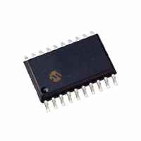
DSPIC33FJ12MC201-I/SO Microchip Technology, DSPIC33FJ12MC201-I/SO Datasheet - Page 103

DSPIC33FJ12MC201-I/SO
Manufacturer Part Number
DSPIC33FJ12MC201-I/SO
Description
IC DSPIC MCU/DSP 12K 20SOIC
Manufacturer
Microchip Technology
Series
dsPIC™ 33Fr
Datasheets
1.PIC24HJ12GP201-ISO.pdf
(84 pages)
2.DSPIC33FJ12MC201-ISO.pdf
(288 pages)
3.DSPIC33FJ12MC201-ISO.pdf
(14 pages)
4.DSPIC33FJ12MC201-IP.pdf
(284 pages)
Specifications of DSPIC33FJ12MC201-I/SO
Program Memory Type
FLASH
Program Memory Size
12KB (12K x 8)
Package / Case
20-SOIC (7.5mm Width)
Core Processor
dsPIC
Core Size
16-Bit
Speed
40 MIPs
Connectivity
I²C, IrDA, SPI, UART/USART
Peripherals
Brown-out Detect/Reset, Motor Control PWM, QEI, POR, PWM, WDT
Number Of I /o
15
Ram Size
1K x 8
Voltage - Supply (vcc/vdd)
3 V ~ 3.6 V
Data Converters
A/D 4x10b
Oscillator Type
Internal
Operating Temperature
-40°C ~ 85°C
Product
DSCs
Data Bus Width
16 bit
Processor Series
DSPIC33F
Core
dsPIC
Maximum Clock Frequency
40 MHz
Number Of Programmable I/os
15
Data Ram Size
1 KB
Maximum Operating Temperature
+ 85 C
Mounting Style
SMD/SMT
3rd Party Development Tools
52713-733, 52714-737, 53276-922, EWDSPIC
Development Tools By Supplier
PG164130, DV164035, DV244005, DV164005, PG164120, DM240001, DV164033
Minimum Operating Temperature
- 40 C
Lead Free Status / RoHS Status
Lead free / RoHS Compliant
For Use With
DV164033 - KIT START EXPLORER 16 MPLAB ICD2DM240001 - BOARD DEMO PIC24/DSPIC33/PIC32
Eeprom Size
-
Lead Free Status / Rohs Status
Lead free / RoHS Compliant
- PIC24HJ12GP201-ISO PDF datasheet
- DSPIC33FJ12MC201-ISO PDF datasheet #2
- DSPIC33FJ12MC201-ISO PDF datasheet #3
- DSPIC33FJ12MC201-IP PDF datasheet #4
- Current page: 103 of 288
- Download datasheet (5Mb)
8.1.3
The primary oscillator and internal FRC oscillator can
optionally use an on-chip PLL to obtain higher speeds
of operation. The PLL provides significant flexibility in
selecting the device operating speed. A block diagram
of the PLL is shown in Figure 8-2.
The output of the primary oscillator or FRC, denoted as
‘F
... or 33 before being provided to the PLL’s Voltage
Controlled Oscillator (VCO). The input to the VCO must
be selected in the range of 0.8 MHz to 8 MHz. The
prescale
PLLPRE<4:0> bits (CLKDIV<4:0>).
The PLL Feedback Divisor, selected using the
PLLDIV<8:0> bits (PLLFBD<8:0>), provides a factor ‘M,’
by which the input to the VCO is multiplied. This factor
must be selected such that the resulting VCO output
frequency is in the range of 100 MHz to 200 MHz.
The VCO output is further divided by a postscale factor
‘N2.’ This factor is selected using the PLLPOST<1:0>
bits (CLKDIV<7:6>). ‘N2’ can be either 2, 4, or 8, and
must be selected such that the PLL output frequency
(F
generates device operating speeds of 6.25 to 40 MIPS.
For output ‘F
tor, the PLL output ‘F
EQUATION 8-2:
FIGURE 8-2:
© 2009 Microchip Technology Inc.
Source (Crystal, External Clock
IN
OSC
or Internal RC)
’, is divided down by a prescale factor (N1) of 2, 3,
) is in the range of 12.5 MHz to 80 MHz, which
factor
PLL CONFIGURATION
Note 1: This frequency range must be satisfied at all times.
IN
’ on a primary oscillator, or FRC oscilla-
F
OSC
‘N1’
OSC
=
F
dsPIC33FJ12MC201/202 PLL BLOCK DIAGRAM
OSC
F
’ is given by Equation 8-2.
IN
is
⋅
CALCULATION
⎛
⎝
------------------ -
N1 N2
selected
M
⋅
⎞
⎠
PLLPRE
Divide by
2-33
N1
using
0.8-8.0 MHz
Here
Preliminary
the
(1)
dsPIC33FJ12MC201/202
X
For example, suppose a 10 MHz crystal is being used
with the selected oscillator mode of XT with PLL.
• If PLLPRE<4:0> = 0, then N1 = 2. This yields a
• If PLLDIV<8:0> = 0x1E, then
• If PLLPOST<1:0> = 0, then N2 = 2. This provides
EQUATION 8-3:
VCO input of 10/2 = 5 MHz, which is within the
acceptable range of 0.8-8 MHz.
M = 32. This yields a VCO output of 5 x 32 = 160
MHz, which is within the 100-200 MHz ranged
needed.
a Fosc of 160/2 = 80 MHz. The resultant device
operating speed is 80/2 = 40 MIPS.
Divide by
PLLDIV
2-513
F
VCO
M
CY
=
100-200 MHz
F
-------------
Here
OSC
2
F
VCO
(1)
=
1
-- -
2
⎛
⎝
PLLPOST
XT WITH PLL MODE
EXAMPLE
Divide by
10000000 32
--------------------------------- -
2, 4, 8
N2
2 2 ⋅
⋅
12.5-80 MHz
DS70265D-page 101
⎞
⎠
Here
=
40 MIPS
(1)
F
OSC
Related parts for DSPIC33FJ12MC201-I/SO
Image
Part Number
Description
Manufacturer
Datasheet
Request
R

Part Number:
Description:
IC, DSC, 16BIT, 12KB, 40MHZ, 3.6V, DIP28
Manufacturer:
Microchip Technology
Datasheet:

Part Number:
Description:
Manufacturer:
Microchip Technology Inc.
Datasheet:

Part Number:
Description:
Manufacturer:
Microchip Technology Inc.
Datasheet:

Part Number:
Description:
Manufacturer:
Microchip Technology Inc.
Datasheet:

Part Number:
Description:
Manufacturer:
Microchip Technology Inc.
Datasheet:

Part Number:
Description:
Manufacturer:
Microchip Technology Inc.
Datasheet:

Part Number:
Description:
Manufacturer:
Microchip Technology Inc.
Datasheet:

Part Number:
Description:
Manufacturer:
Microchip Technology Inc.
Datasheet:

Part Number:
Description:
Manufacturer:
Microchip Technology Inc.
Datasheet:


